


Contents

On-demand webinar
How Good is My Shield? An Introduction to Transfer Impedance and Shielding Effectiveness
by Karen Burnham
Schematic and netlist checks are performed to check schematic symbols, verify electrical characteristics, and analyze the netlist consistency.
A PCB schematic refers to a simple two-dimensional circuit design representation displaying the functionality and connectivity between different components. It shows how the components are electrically connected. The output of a schematic is a netlist and a BOM.
This article focuses on how to have an error-free schematic design and explains various schematic, netlist, and BOM checks.
Schematic design flow
Schematic generation consists of the following steps:

Creating schematics
When you are creating a schematic, it is important to make sure you are illustrating the circuit with specific steps.
Here are the standard schematic guidelines:
- Page size selection: Different design tools offer different page sizes. In general, the page size is kept as A4.
- Naming and editing the schematic symbol: Name the logical blocs of the schematic as A, B, C. They can be used to label the pages. In this way, the pages can be arranged in alphabetical order and separated. For ex:
- A_Block diagram
- B_Power supply
- Symbols can be added in the component to different positions of the pin. It represents the electrical information of the pin.
- Grid setting: The grid helps you to indicate the parts properly and ensures a solid connection of components on the grid.
- Blocks and comments: Fill in the required details such as page size, document, and name/function of the circuit. The notes can be written on documents or schematic pages.
- Configuring pin properties: Since a pin has several properties, including a name and a designator, it can be configured on the schematic of the preferences dialog.
- You can utilize the schematic library panel to create symbols.
- Components can be created with the design objects in the schematic library editor. They can be copied and pasted from one library to another or the schematic library editor.
- Every schematic check must have proper net connections.
- After placing the components, design rule check and netlist format verification are carried out.
What is a schematic symbol?
A schematic symbol is a simplified representation of a component. Each symbol contains a graphic or drawing that represents its part or function.

They constitute the building blocks of typically rectangular or square shapes consisting of numbered pins and pin names of any electrical schematic. The symbolic representation of an electrical component displays its respective connection points. The standards of electrical design symbols are ANSI and IEC.
The schematic symbol represents physical components that can be soldered to the circuit board during the assembly process. It may also display PCB structures like vias or test points. The symbol will also be associated with a component name and sometimes the footprint.

PCB Design for Assembly Handbook
6 Chapters - 50 Pages - 70 Minute ReadWhat's Inside:
- Recommended layout for components
- Common PCB assembly defects
- Factors that impact the cost of the PCB assembly, including:
- Component packages
- Board assembly volumes
Download Now
What is a net on a schematic?
A net refers to a connection between two or more interconnected components. The netlist conveys the connectivity information, while its structure, complexity, and representation can vary.
Net nomenclature
A net name uniquely identifies net connections between components.

What is a schematic netlist?
A schematic netlist is important information in design software to create a real PCB. It has nets with labels and a list of all the components connected to that net. It also contains information regarding components, their designators, pins, and the names of any nets that connect each pin to components.
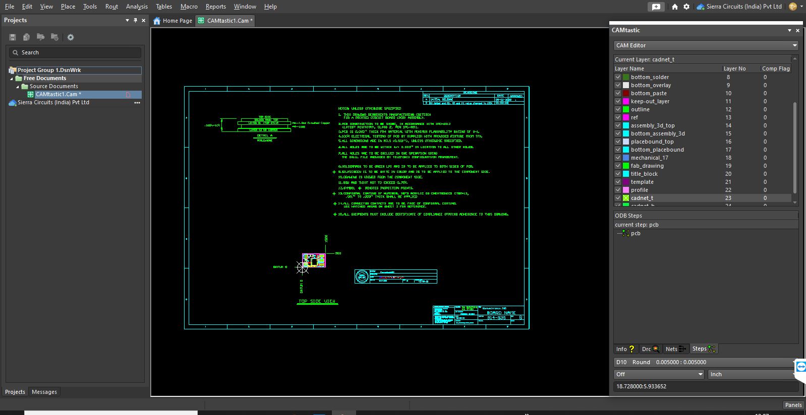
A netlist depicts every net in the schematic and the connections circuit board nets make between components. Every electrical computer-aided design (ECAD) software program is used to write a circuit board netlist. You can extract the netlist from your design and view it in ASCII format using a text editor.
- (RESET0 C49-2 R35-1 U15-10 U17-1)
- Here, RESET0 represents a net in a netlist connected to capacitors C49 pin 2 and R35 pin1.
- The components in the PCB netlist are represented below:
- [
- C44
- C0603
- 100nF
- ]
- C44 is the capacitor with a value of 100nF and a footprint size of 0603.
Different schematic tools will have different board nets and component formats.
What does a netlist include?
The netlist format can vary widely in terms of the amount of information. The following details must be included in a netlist:
- Reference designator: These designators/component identifiers are for the components connected to the net.
- Pin number: Each component on a net will have some pins, hence the pin will appear in the netlist.
- Netlabels: The name you give to a particular net in your schematic.
After you finish the schematic capture, the netlist can be utilized to create the connecting lines in an unrouted layout.
These nets are called rat nests and represent the shortest distance between two pins.
If you don’t want to make any further changes to the schematic, then the design data remains consistent as you route the board.
Need help building a schematic and netlist library? Our engineering team can assist you with schematic review, netlist verification, connectivity checks, and design validation to catch issues early and avoid costly respins.
You can book a meeting with our experts or call us at +1 (800) 763-7503.

Generation of netlist using Altium Designer
- Netlist can be generated on Altium Designer by selecting Design> Netlist > Create netlist from the connected copper command.

- A confirmation dialog will appear for netlist creation.

- Click on “Yes”. A new netlist is created and gets automatically opened as the active document.

- Every net in the netlist derives its name from one of the pads connected to the routed copper.
Generation of netlist using Orcad Capture
Generation of netlist using Orcad Capture follows the below-mentioned steps:
- Select Tools> Create netlist from the menu.
- With the PCB tab selected, check to Create PCB Editor Netlist.
- Browse the location to save.
- If this is the first time, then select Setup.
- Browse to the location of the allegro.cfg file.
- Click OK to close the setup.
- Click OK to netlist design.
Netlist checks
Netlist check is an important design verification step that is done manually.
To begin with, export the netlist from the layout and manually crosscheck this with the schematic file. This will eliminate the following errors:
-
- Design errors – Connection errors like wrong pin connection. Always verify the pin configuration with the datasheet.
- Net label errors – Carefully name the nets. For instance, RESET 0 and RESET0, which are the same signal names, will not connect since the former has a blank space between T and o, which can be referred to as typography errors.
- Single-ended nets – Nets that are labeled but are connected to one single pin. For example, if you name a net as RESET o, but the other end of the connection has a different net name, then it will lead to a floated connection or an open connection.
During a netlist check, every connection in the schematic and layout is checked with each net in the netlist.

Schematic verification in Altium Designer
Schematic verification is implemented while exporting the bill of materials or the netlist.
Following are the steps to carry out the schematic checks using Altium Designer:
- To check the design, select Project > Validate PCB Project name.
- The software checks for logical, electrical, and drafting errors between the unified data model and project-checking settings.
- Validated design undergoes several drafting and electrical checks.

Drafting checks
After verification, you can check the errors and warnings in the Error Reporting tab, as shown in the below image.
There will be various violations associated with connected nets, components, etc. Every violation’s report mode can be changed to one of the four values by clicking on it and selecting the desired value in the drop-down.

Connectivity checks in Altium Designer
The electrical connectivity is verified by selecting the connection matrix tab.
This matrix offers a great mechanism to establish connectivity rules between component pins and net identifiers. It refers to the logical or electrical conditions which can be reported directly as warnings or errors.

ERC checks
The ERC checks are conducted to suppress all the reported electrical rule check warnings or error violation conditions that are detected during the compilation of the schematic layout project. For conducting an ERC check, you can follow the given steps in Altium Designer:
- Open an Output job file.

- Under validation outputs, you can add new validation.
Then select Electrical rules check from the drop-down.
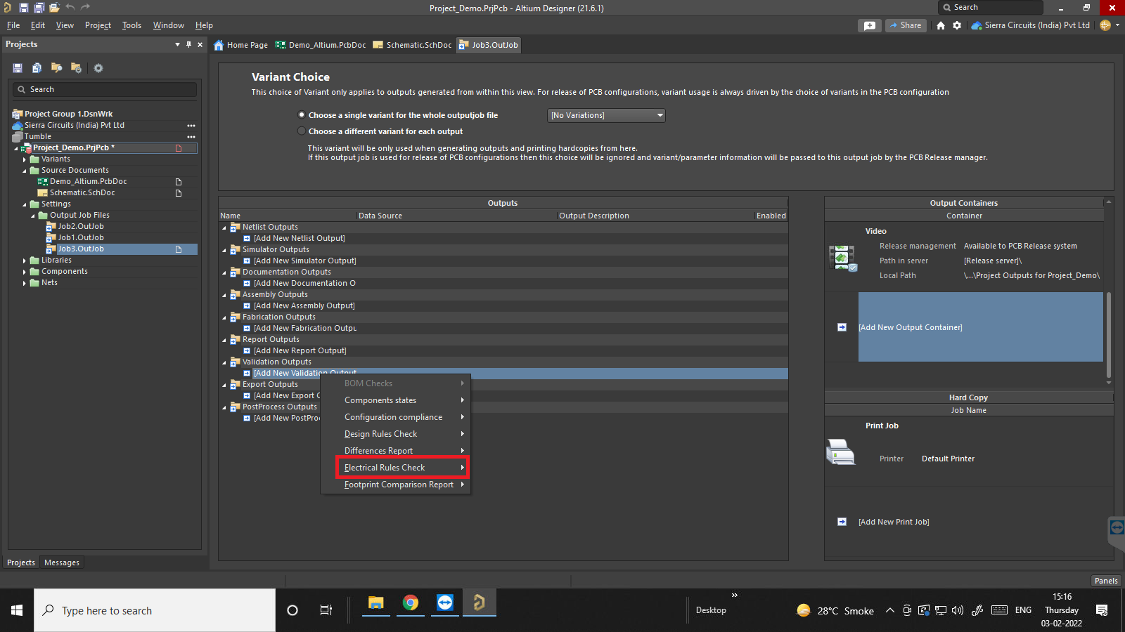
From the obtained results, you can select the schematic document.
- Right-click on the newly added ERC entry and click Configure.
- Validation – As a part of the validation, you can use the drop-down to define the maximum tolerated error level while using the ERC output generator. The validation stage of the release process flow utilizes the checks defined only in the output job and not the project-level ERC check. Hence you can define various sets of checks, to ensure higher integrity of the design data.
- Suppressed errors – This option reports any suppressed errors in the schematic.
- Show columns – You can select the columns to be displayed in the ERC report. Select the options such as class, document, and message. As the selections are made, the preview region is updated to show the column settings.
To learn about via placement settings, via constraint settings, etc., read PCB via design using Altium Designer.
Error reporting tab
The error reporting tab enables you to define the reporting levels for each of the possible violations that exist on schematic layout documents when compiling the project. These violation settings will be used with the connection matrix tab to test the source documents for violations. If any violations are found, then the warning error or fatal error will be displayed as violation messages in the panel.
Violations grid
This region presents every possible violation on the project’s source documents. It includes:
- Violations associated with buses, components, configuration constraints, and parameters.
Each specific violation type is presented with the following fields:
- Violation type description- mentions a short description of the violation type.
- Report mode- uses the field to specify the levels associated with violating the checks.
BOM
A bill of materials is a comprehensive list of parts, items, assemblies, subassemblies, documents, and other materials required to create a product. It is important to create an accurate BOM, especially when handling the assembly job at an assembly house.
The BOM file is generated through a dedicated report generation engine in the schematic software. This is the phase referred to as the report manager.
Creating a BOM in Altium Designer
Select Reports> Bill of Materials option from the schematic or PCB editor. In each case, the source document can be easily compiled, followed by a display of the report manager dialog.

The dialog box presents various properties for all components of the source documents. Every document has its own column. It simply selects which data to be included in the generated BOM report. Data can be grouped and sorted according to the requirement. It also has the ability to include additional data from a nominated PCB for the project.
You can download Sierra Circuits’ preferred BOM template.
The required information for a bill of materials is:
- Quantity per board
- Manufacturer part number (MPN)
- Do not install parts (DNI)
- Reference designators assigned to each part
- Vendor name (optional)
- Vendor part number (optional)
- Value (optional)
- Size/footprint (optional)
- Part description/specs (recommended)
- Manufacturer name (optional)
The BOM verification should be done for the following:
- Duplication of reference designators
- Comparison of reference designators with their mentioned quantity
- Duplication of manufacturer part numbers
- Incorrectly specified range of reference designators
- The description of the part does not match the MPN
Bill of materials creation choices
The report manager can generate the final BOM in various output formats like PDF, CSV, Excel, HTML, or XML. The preferred format is an Excel sheet.
Exporting the BOM in Altium Designer
- After the content for the BOM is defined, the reports can be generated.
- The export options region of the report manager is used for exporting this data.
You can export the bill of materials and perform the following steps:
- You can select the format for exporting the data and utilize the File format drop-down menu.
- .CSV (Comma Delimited)(*. CSV)
- Tab-delimited text(*.txt)
- MS Excel( *.xls, *.xlsx) uses Microsoft Excel
- Generic XLS (utilizes a built-in format file generator so that this format can be generated without the installation of Microsoft Excel)
- Portable document format(* .pdf)
- Web page ( *.htm, *.html)
- XML spreadsheet(*.xml)
- An Excel template can be easily applied to the exported data if the export format is in Excel.
- Enable the open exported option to access the exported file in the associated software application.
- Enable the Add to Project to get the generated report after its creation.
- You can enable the report BOM violations in messages to make a quick check for the active BOM during the generation.
- Click on Export to specify the places where the report needs to be saved.

Common errors in BOM
- Incomplete MPN- Sometimes, the part number is not complete, which could result in the selection of wrong footprints for components.
- Wrong values of components- Check all the values of components, especially resistors, capacitors, their voltage ratings, values, tolerance, and power ratings.
- Obsolescence of components
- Components out of stock
For error-free designs, a schematic that would generate netlist and BOM is essential. We have highlighted the need to carry out ERC netlist checks and BOM checks before proceeding to layout designs.
Have questions on schematic design? Post them on our forum, SierraConnect. Our PCB experts will answer your queries.


