PCB layout design starts with a schematic, and is later materialized by a custom manufacturer like Sierra Circuits. The schematic serves as a blueprint for laying/routing the traces and placing the components on the board. A PCB editing software is used to import all of the components and footprints into a board file. Each schematic symbol needs to have a footprint associated with it.
What is PCB layout design process?
The actual design process starts by converting an electronic product design idea into a schematic diagram followed by a physical circuit board layout. During the initial design phase, functional requirements are essential since they act as input for the schematic, stack-up design, footprint generation, and layout design. The information gathered while finalizing the layout acts as input for board manufacturing, assembly, and testing. After achieving a specific shape and size of the board, designers use a layout software for component placement and electrical connectivity called routing. An ideal circuit design should meet the stringent DFM/DFA checks.
Beat competitors to the market. Reduce Respins with our Zero-Defect Guarantee.
With Turnkey PRO, Sierra Circuits delivers full turnkey PCB assemblies guaranteed to work.
Designing a board layout
Before starting with the layout, the stack-up must be designed. During the stack-up design, manufacturers decide the best technology would be suitable from an optimization point of view. For a detailed perspective of layout design see how to design a PCB layout.
Board design planning
Planning a circuit design is the most critical phase since it requires the type of components to be used, their placement, identifying the critical signals, power requirements, etc.
What are schematics in a board design?
Schematic capture is the first step for designing a neat and logical PCB. A schematic diagram uses abstract and graphic symbols to logically represent the elements of a system. It signifies how the components are connected.
Schematics can be drawn from specifications, marked-up schematic sheets, and block diagrams. A netlist depicts the electrical connection from node to node present in the schematic. We accept schematics in any format (PDF and sketch.) and can convert them into a preferred CAD format.
Adding notes while creating a schematic diagram can be very helpful during the PCB layout design. For example, a note like, “this pin requires a guard track to signal ground”, helps the person laying out the board what precautions must be taken. Schematic notes are also useful for people reviewing the board design.

High-Speed PCB Design Guide
8 Chapters - 115 Pages - 150 Minute ReadWhat's Inside:
- Explanations of signal integrity issues
- Understanding transmission lines and controlled impedance
- Selection process of high-speed PCB materials
- High-speed layout guidelines
Download Now
What are PCB footprints?
Footprints are the pattern on which the electronic components are mounted and soldered. They define the component’s physical dimensions and placement of the copper pads or through holes. Footprints of components are required during the layout stage. Thus, it is necessary to create them before you start with your design.
They give an idea of the actual size of the component and assist in an efficient realestate planning.
Factors to be considered in a board layout
PCB layout design involves marking the board outlines, setting up the constraints of the circuit board, placing the components, routing, and generating the production files, etc. Component placement and routing requires expertise and thorough understanding of the circuit.
Component placement
Component placement required strong problem-solving skills since they need to be placed with accuracy. It will make your layout job easier and ensures the best electrical performance. If there are some major errors, it can turn your routing job into a nightmare and results in poor electrical performance.
Each designer has his own way of placing components. The same circuit can be designed in 100 different ways by 100 different layout designers. So, there is no right way to place your components. But there are quite a few basic rules which will ease the routing process and give the best electrical performance.
- Set snap grid, visible grid, and default track/pad sizes.
- Drag all the components onto the board.
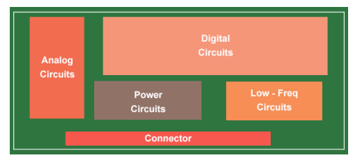
- Divide and place your components into functional building blocks, wherever possible. The circuit can be divided into functional blocks such as power supply, controller, and analog sensors, etc.
- Place the connectors as main components or as specified by the customer.
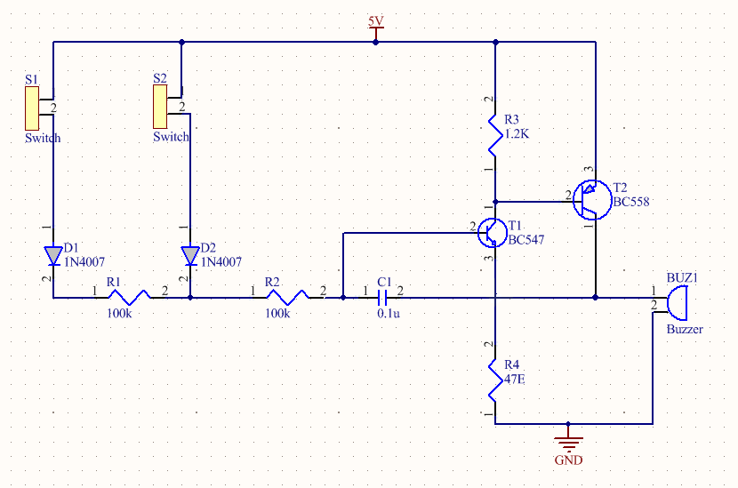
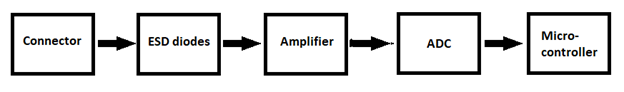
- The components should be placed in the flow of the signal. For example, in a temperature and sensor circuit, first the connectors are placed as specified by the designer/engineer. Then, the ESD protection diodes are placed close to the connectors. Next the signal amplifier circuit is placed. In case there is an external ADC, it should be placed after the amplifier. The signals from the ADC then flow into the microprocessor.
- Separate the digital and analog circuits so that there is no interference in the analog signals.
Routing/tracking rules
Routing is a process of connecting different parts of the circuits such as component pins, resistors, capacitors, etc., with copper traces to complete a circuit. This helps to carry a signal, such as voltage and current, from one part of the circuit to another. One fact is worth noting here that two circuit boards can never be the same. It is routing that makes your design unique.
- Identify critical tracks on your circuit and route them first.
- Place the ground and power vias next to the component pins.
- Place and route each building block separately.
- Route rest of the signals between blocks.
- Keep nets as short as possible. Because a longer track leads to greater resistance, capacitance, and inductance.
- Avoid right angles in tracks, and implement 45 degrees angles only. PCB packages come with a mode to enforce 45-degree movements. Make use of it.
- Route the tracks in an orthogonal manner, not just point to point. Point to point tracking is not space-efficient if you want to lay more tracks on other board layers.
- Enable your electrical grid, also called ‘snap to center’ or ‘snap to nearest’ option. Place the tracks on the grid as a rule. Let your design software find the centers of pads and ends of tracks automatically for you.
- Always take your track to the center of the pad, don’t make your track and pad ‘just touch.’ Otherwise, your software program will not consider it as an electrical connection to the pad.
- Do not use multiple tracks pinned together end to end. Use a single track to avoid future editing issues.
- Ensure that tracks pass through the exact center of pads and components. Use the correct snap grid to get it done. If your track doesn’t pass through the exact center, it means you are using the wrong snap grid. The correct snap grid makes your board more elegant and symmetrical. It gives the most clearance.
- In the case of circuits with high currents, use multiple vias when going between layers. It will reduce track impedance and improve reliability.
- Impedance value (depends on the trace width) is important to consider in high-speed routing. We use the Instack tool for impedance calculations and stack-up.
- For effective bypassing and reduced loop inductance, keep power and ground tracks close to each other. Don’t lay them in opposite directions around the board.
- Keep routing and component placement symmetrical.
- Don’t leave any ground copper fills unconnected. Do not forget to ground them.
- Perform a design rule check (DRC) and get it verified.
Sierra Circuits’ engineers and technicians have the experience to bring your PCBs to life.
Start an online quote now.
How to improve your printed circuit board design
Any design can be improved by keeping the following critical aspects in mind. It will not only help the designers but the manufacturers too.
- Measurement units: The first thing about PCB design is to know the measurement units used and their common terminologies. As a general rule, use ‘mils’ for basic design and layout requirements such as tracks, pads, spacings, and grids. And use ‘mm’ for mechanical and manufacturing requirements such as hole sizes and board dimensions.
- Working on grids: It is one of the significant rules of circuit board design that beginners generally overlook. It is all about laying out your board on a fixed grid called ‘snap grid.’ This helps you fix the cursor, components, and tracks into grid positions.
Grids make future editing, dragging, movement, and alignment of your tracks and components easier, as your layout grows in size and complexity. It also keeps your components neat and symmetrical. Some of the advanced PCB design softwares come with hotkeys to switch between different snap grid sizes.
- Top to bottom approach: It is also called “through the board” approach, where you have to get used to reading text on the bottom layers as mirror images. It is like looking from the top of the board, through the various layers as if they are transparent. You only look at the board from the bottom during manufacturing for verification purposes.
- Track size: We cannot follow a set standard for track sizes. Since the track size depends on the electrical, routing space, and clearance requirements of PCB design. Every design has a different set of electrical requirements that can be fulfilled by changing the track’s size. All board designs require a mixture of different track sizes, and their requirements cannot be met by following a fixed size.
A bigger track has lower DC resistance and inductance. Such tracks are easier to etch, inspect, and rework. In general, the current carrying capacity of any track is related to its width, and the maximum temperature rise your manufacturer is willing to consider. It is always the fabrication’s call to decide the lower limit of the track as it depends on the trace and space resolution.
Every track on a circuit board acts as a resistor, and hence it dissipates heat. As the width of the track increases, the resistance decreases. Check our trace width and current capacity calculator.
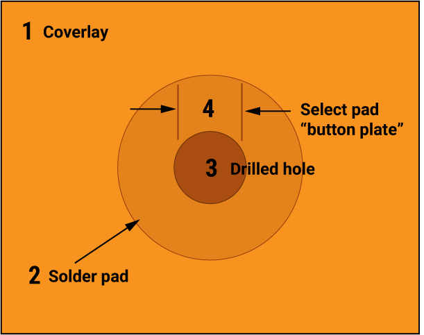
- Pad size and dimension: Pad sizes, shapes, and dimensions depend on the component in use and the technique used to assemble the board. The layout software comes with a set of basic component libraries, and you can modify these component libraries to suit your purpose.
Pad/hole ratio is an important parameter in this context. It is the ratio of the pad size to the hole size, and manufacturers have their own minimum specification for this. Generally, the pad should be at least 1.8 times the diameter of the hole, or at least 0.5mm larger. This proportion is critical when the pad and hole are smaller since it allows for alignment tolerances on the drill and the artwork on top and bottom layers. The minimum via size is determined by the aspect ratio. It is 10:1 for through-holes.
- Vias and through hole pads: Vias electrically connect the tracks from one layer of the board to another. In general, the via holes are plated through holes. Now the question is, are there any differences between via and through hole pad? Practically, there is no difference. Both via and through hole pads are just electrically plated holes. They are different when it comes to PCB design software. Through hole pads and vias should be treated differently. While using a different design package, you can edit them separately. So, it is not advised to use a through hole pad in place of a via and vice-versa.
- Polygon: A polygon is used in many board design packages. It is used to fill the desired area with copper that flows around other pads and tracks. They are handy for laying down ground planes. Place the polygons after placing all the tracks and pads. Polygons are of two types: a solid fill of copper and hatched copper tracks arranged in a crisscross fashion. Nowadays, solid fills are preferred over hatched fills.
- Clearances: Electrical clearances are also important for all circuit boards. Too tight clearance between tracks and pads may lead to hairline shorts and other etching problems during the manufacturing process. It is very hard to find fault once a board is assembled. It is not recommended to push the limits of the manufacturer unless you have to. It is good to stay within their recommended minimum spacing if possible.
- User interfaces: The location of components like power connections, potentiometers, LEDs, and audio jacks in the finished project also affects how a PCB is laid out. Hence, it is best to design the rest of your circuit board by keeping these component locations in mind.
How to design flex boards
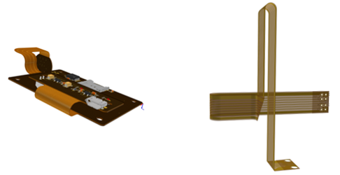
- Flex cycles: A flex circuit is made from a very thin yet strong enough substrate to survive multiple flexing cycles while carrying signal and power continuously.
- Define circuit parameters based on the application: Use a paper arrangement to represent the circuit. Experiment with bending and forming the paper template to optimize shape and fit. While designing the final shape, consider how the circuits are laid out on a processing panel. If there are more circuits per panel, the cost will be lower.
- Layer count mismatch in the PTH area: Areas that have plated through holes should have the same layer count and construction.
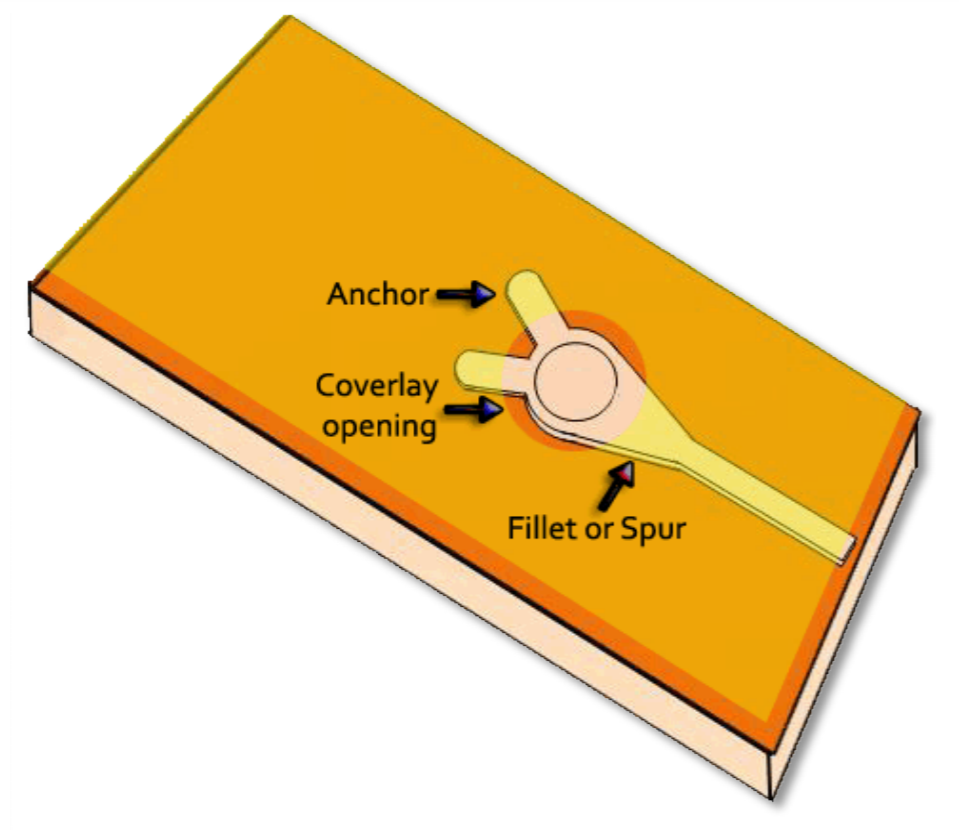
- Feature size: Since flex circuits are inherently unstable in nature, small features (i.e., via pads) can result in processing problems and fewer yields. Also, ensure that vias are tear-dropped and anchors and/or tabs are added. Make the annular rings as large as possible.
- Aspect ratio of the conductor: Conductors should be designed with a width equal to at least five times the thickness. For example, with 2oz copper (0.0028 inches/50μm), the conductors should be 0.0140 inches (0.36mm) or wider.
- Vibration resistance: Flex boards can withstand shock and vibrations and thus less repair and replacement cost.
- Termination option supports: PCB connectors, FFC connectors, and insulation displacement connectors are accepted by flex circuits. They also support several options, like unsupported fingers, which can only be done on flex.
Quick points for the designers
- Maintain a balance between the conductor weights and material thickness on each side of the neutral bend axis.
- Flexibility can be improved by implementing staggered conductors from layer to layer. Stacking conductors on top of each other on multiple layers result in a thicker and stiffer circuit. It is also called the I-Beam effect that needs to be avoided.
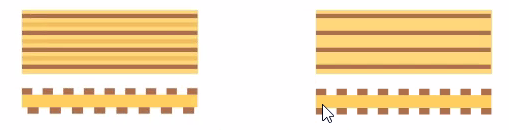
In the above image, the left section is depicting the stacked conductors and the right section is showing the staggered conductors.
- Route conductors perpendicularly as possible through bend areas.
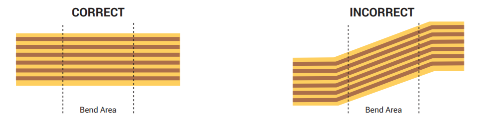
- Conductor thickness and width should remain uniform in bend areas.
- Add stiffeners under termination areas to remove the stress around them.
- Avoid plated through-holes in the bend areas.
- In flex boards, use arc routing. And, the annular ring for the plated hole should be more compared to rigid boards.
- If the circuit has to bend within 1 inch (25.4mm) of termination pads, fillets are placed at each conductor/pad interface. Stress generated should not impact the immediate bend area but should radiate out from the bend.
- Use a cross-hatched pattern rather than solid copper, if shields or ground planes are needed.
- Utilize tear stops or reliefs for slits in the circuit.
- If bend reliability needs improvement, then unbond the flexible substrates from each other. The substrates in the unbonded area come with lower thickness compared to the total circuit, hence tighter bends are possible. This method is called the loose leaf method.
- Remove copper plating from the conductors in the flex area by using selective (pads-only) plating.
It is quite difficult to try and teach PCB design. There are many basic rules and good practices to follow, but board design is a highly creative and an individual process. It is like trying to teach someone how to paint a picture. Everyone will draw and paint in their unique style.
Try our free Better DFM tool and save time and money. Our automated platform will catch any PCB design error ahead of time and prevent on-holds and re-spins.
Get started by uploading your Gerber files here.


