


Contents
PCB trace width determines how much current a conductor can safely carry without excessive heat buildup, voltage drop, or reliability issues. Parameters such as copper thickness, temperature rise, trace location, and conductor cross-sectional area directly influence a trace’s current-carrying capacity.
Designing high-current boards presents challenges such as balancing current requirements with board space constraints, managing heat generated by power traces, and ensuring reliable current distribution across layers and vias.
In this article, you’ll learn how PCB trace width affects current-carrying capacity, the key considerations for high-current circuit board design, practical layout guidelines for handling large currents, and how trace width calculators help determine the optimal conductor dimensions.
Highlights:
- High-current board designs use wider traces, heavier copper weights, polygon pours, and copper bus bars to support increased current demands.
- Thermal management techniques such as minimizing trace length, isolating heat-sensitive components, and optimizing copper distribution improve board reliability.
- PCB trace width calculators based on IPC-2221 and IPC-2152 guidelines help designers accurately size traces for safe and efficient current flow.
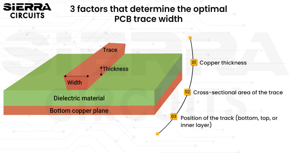
What parameters determine the required PCB trace width?
The appropriate conductor width depends on the trace’s current-carrying capacity, which is influenced by copper thickness, trace cross-sectional area, and whether the trace is on the top, bottom, or inner layer.
PCB trace width refers to the horizontal dimension of a copper trace, while trace thickness refers to its vertical dimension.

A trace or track is a copper conductor on the board that conducts signals on the surface of the board. It is the flat, narrow portion of the copper foil that is left behind after etching.
The electricity that flows through the copper traces generates a significant amount of heat. Correctly calibrated trace width and thickness help minimize the buildup of heat in your board. The wider the track, the lower the resistance to current, and the less heat is built up.
Circuit board design often starts with a default trace width, but this value may not be suitable for every application. The appropriate width should be determined based on the current-carrying capacity of the trace.
There are several factors to consider when determining the right trace width:
- Copper layer thickness: Copper thickness is the actual trace thickness on a printed board. The default copper thickness for high current PCBs is around 1oz (35 microns) to 2oz (70 microns)
- Cross-sectional area of the trace: Higher power requirements on a circuit board require traces with a higher cross-sectional area. This is directly proportional to the trace width.
- Position of the trace: Bottom, top, or inner layer
To learn how to design efficient traces, download the PCB Trace and Space Handbook.
PCB Trace and Space Handbook
8 Chapters - 34 Pages - 40 Minute ReadWhat's Inside:
- Key factors influencing line width and spacing
- Clearance guidelines for high-voltage and high-speed traces
- DFM rules for heavy copper PCBs
- Via considerations
- Industry standards for trace and space design
Download Now
How do you design a high-current circuit board?
High-current circuit boards are typically designed by increasing the width and thickness of copper traces, often to 2 oz. However, this approach increases the board area and may require additional layers.
Digital, RF, and power circuitry mostly process or transfer low-power signals. These applications have copper weights from 1-2 oz and carry current from mA to 1 A or 2 A. Some applications, such as motor controls, require currents up to 50A, which will require higher copper weights on the PCB and larger trace widths.
The cross-sectional area of the trace impacts the via current-carrying capacity. In such a case, increasing the trace width will achieve a proper current rating.

8 layout strategies for designing high-current PCBs
High-current board design involves optimizing trace widths, minimizing trace lengths, improving heat dissipation, and creating low-resistance current paths using techniques such as polygon pours, internal copper layers, via stitching, and copper bus bars.
The following guidelines can help improve the performance of high-current designs.
1. Keep high-current traces short
Longer traces have higher values of resistance and also carry higher currents, leading to larger power loss. Since the power loss generates heat, board life will be reduced. Therefore, it is critical to keep traces carrying large currents as short as possible.
For high-current trace design strategies, see 10 layout tips for high-speed and high-current PCB traces.
2. Calculate the trace width based on temperature rise
Trace width is a function of variables like the resistance and current through it, along with the permitted temperature rise. Conventionally, a temperature rise of 10°C is allowed above the ambient temperature of 25°C.
In case board material and design permit, it is even possible to allow for a 20°C temperature rise. You can see how we have designed our traces to allow different operating currents in our case study on designing a high-current PCB with voltage doublers.
To learn more about efficient thermal management of traces, read our blog on how to optimize your PCB trace using the IPC-2152 standard.
3. Thermally isolate heat-sensitive components
Some electronic components, like voltage references, analog-to-digital converters, and operational amplifiers, are sensitive to temperature changes. When such components are subjected to heat, their signal can change.
High-current boards are known to generate heat; the components mentioned above need to be thermally isolated to a certain level from the hotspots. You can do this by having board cutouts and providing thermal relief connections.
4. Remove solder mask from current-carrying traces
To increase the current capability of a trace, you can remove the solder mask, which exposes the copper underneath. Then additional solder can be added onto the trace, which will increase its thickness and reduce resistance. This will allow more current to flow through the traces without an increase in trace width or incurring the costs of additional copper thickness.
5. Use polygon pours under high-current components
Field Programmable Gate Arrays (FPGAs) and processors come in ball grid array (BGA) and line grid array (LGA) packages and have high current requirements. To enable high current flow, you can have square polygon pours right under the chip and then have vias drop down and connect to them. You can then link the polygon pour to thick power traces or power planes.

6. Utilize internal layers for current distribution
When there isn’t space on the outer layers of a PCB for thick traces, you can have a solid fill in an internal board layer. Next, you can use vias to link to high-current devices present on the outer layers.
For DFM tips, see Design for Manufacturing Handbook.

Design for Manufacturing Handbook
11 Chapters - 96 Pages - 90 Minute ReadWhat's Inside:
- Annular rings: avoid drill breakouts
- Vias: optimize your design
- Trace width and space: follow the best practices
- Solder mask and silkscreen: get the must-knows
Download Now
7. Add copper bus bars for currents above 100 A
In electric automobiles and high-power inverters where the current exceeds 100A, copper traces might not be the best way to transmit power and signal. In this case, you can use copper bus bars that can be soldered onto PCBs’ pads. Copper bus bars have a much higher thickness than traces and can carry high currents as required without any heating issues.

8. Implement via stitching for multi-layer current paths
When a trace is not able to carry the needed current in a single layer, the trace can be routed on multiple layers and be subjected to via stitching linking the layers. This will increase the current-carrying capacity in cases where the trace thickness is the same on both layers.

Sierra Circuits fabricates and assembles high-quality circuit boards in the United States. Visit our PCB manufacturing capabilities to learn more.
Why should you use a PCB trace width calculator?
Manually evaluating the parameters that influence conductor width and applying IPC standards can be time-consuming and error-prone. A PCB trace width calculator simplifies this process by considering factors such as copper thickness, trace length, and location to quickly determine the appropriate value.
According to the IPC-2221 generic standard on printed board design, PCB trace current limits can be classified further into internal and external conductors.
The graphs given below show the relationship between different variables related to trace width. The variables are trace cross-sectional area, temperature rise, and maximum current-carrying capacity for external conductors and internal conductors.


Based on the graphs, a formula to calculate the PCB trace current-carrying capacity is given below:
I = K ΔT0.44A0.75
where,
K = 0.024 for internal conductors and 0.048 for external conductors
ΔT = Maximum temperature difference in °C
A = Cross-sectional area of copper trace in mil²
I = Current carrying capacity in Amperes
Sierra Circuits’ Trace Width, Current Capacity, and Temperature Rise Calculator accurately computes the line width (internal and external) based on electrical load, thermal requirements, and real-world board conditions.
The existing printed board trace width calculators are still based on the data in the graphs and the formula that is given above. They serve as handy tools for PCB designers to calculate trace width with great accuracy. The maximum current-carrying capacity for 2oz copper with a temperature rise of 10°C is mentioned in the table below.
| Maximum PCB trace current capacity (amps) | Minimum trace width for external layers (mil) | Minimum trace width for internal layers (mil) |
|---|---|---|
| 2 | 19.95 | 20.03 |
| 4 | 66.59 | 66.86 |
| 6 | 134.78 | 135.34 |
| 8 | 222.28 | 223.21 |
| 10 | 327.68 | 329.05 |
Need help in designing your PCBs? Our engineering team can assist you with layout design, trace width calculations, material selection, and IPC-2152 compliance to ensure your design handles current loads reliably.
You can book a meeting with our experts or call us at +1 (800) 763-7503.

While determining trace current capacity, there are complex factors at play. However, PCB designers can count on the reliability of trace thickness calculators to help design their boards efficiently. Getting the trace width and its current carrying capacity right can go a long way in designing boards that are reliable and high-performing.
Have queries on designing your next boards? Post them on our community, SierraConnect. Our design experts will answer them.


Start the discussion at sierraconnect.protoexpress.com