


Contents
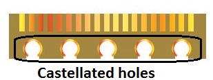
Castellation is a technique used by PCB manufacturers to achieve efficient board-to-board connections. Using this approach, you can integrate multiple castellated circuit boards into a single assembly.
For example, individual modules, like WiFi and Bluetooth, can be mounted together in any given system. The boards are fabricated with semi-plated holes on their edges known as castellated pins. These pins configure the electrical connection of a sub-module to the main board. This can significantly reduce the overall size of the board by eliminating the usage of pin connectors.
How to design a castellated board in Altium Designer
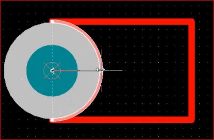
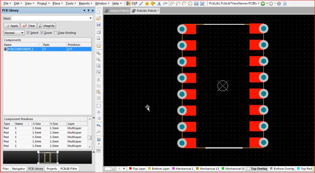
Let us see the steps involved in designing a castellated board with a finished hole of 0.7 mm, a pad-to-pad distance of 2.54 mm, and a pad diameter of 1.5 mm.
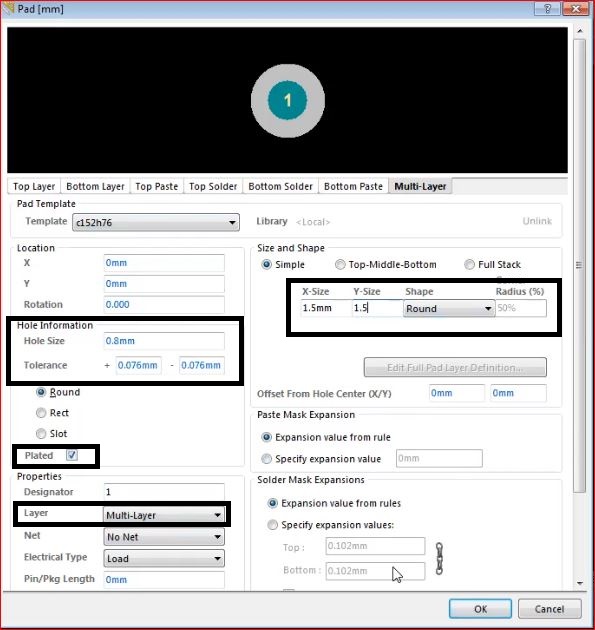
1. Click on Pad from the toolbar and place a dummy pad with a diameter of 1.5 mm.
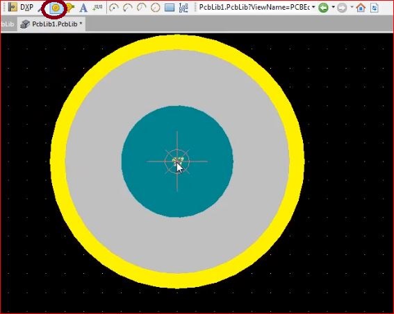
2. Select the dummy pad and set the following dimensions:
- Hole size = 0.8 mm
- Tolerance =0.076 mm
- X-size = 1.5 mm
- Y-size = 1.5 mm
3. Now click on Line, and place the trace with a width of 5 mils.
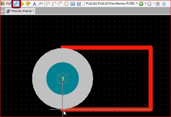
4. Select Arc(Edge) under the option Place and have the arc on the circumference of the pad.
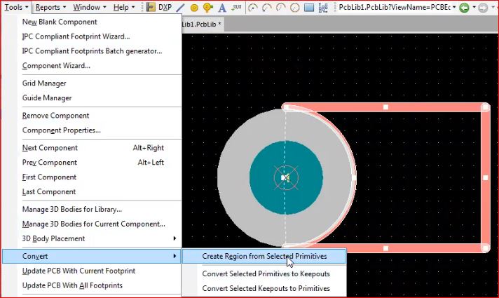
5. Now select the pin structure, go to the Tools tab and choose Create Region from Selected Primitives under Convert.
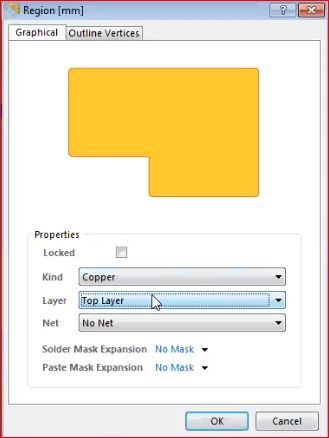
6. To arrange the board layers, double-click on the selected region, arrange them in the following folder:
- Top layer
- Bottom layer
- Top paste
- Bottom paste
- Top solder
- Bottom solder
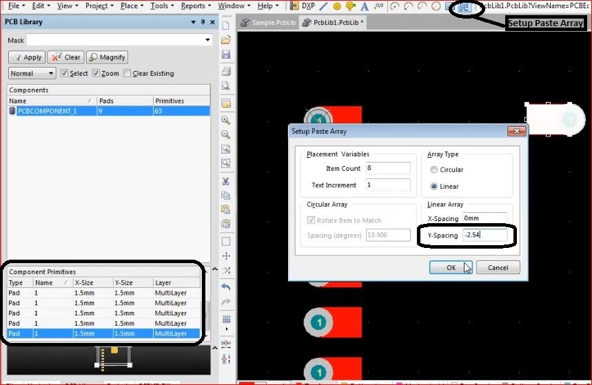
7. After the layer arrangement, click on the Setup Paste Array. This pops up a window asking you to enter the number of pads. You can define it in the item count section. Enter the pad-to-pad spacing in the linear array section as 2.54 mm.
8. The castellated holes are now created on the edge of the board. To align them, go to Edit, select Set Reference and choose Center.
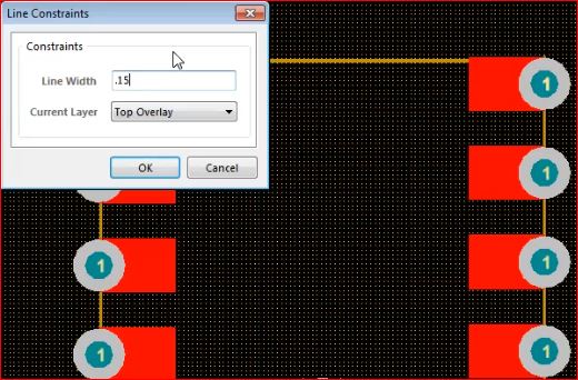
9. Draw the assembly outline and set the line constraint (Line width= 0.15 mm).
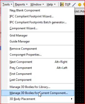
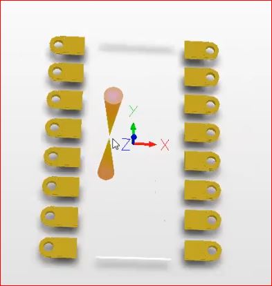
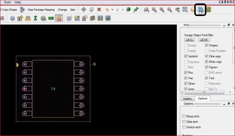
10. To see the 3D view of the board, go to Tool, and select Manage 3D bodies for Current Component.
You can now examine all the layers and sides of the board in 3D.
How to create a castellated board in Allegro
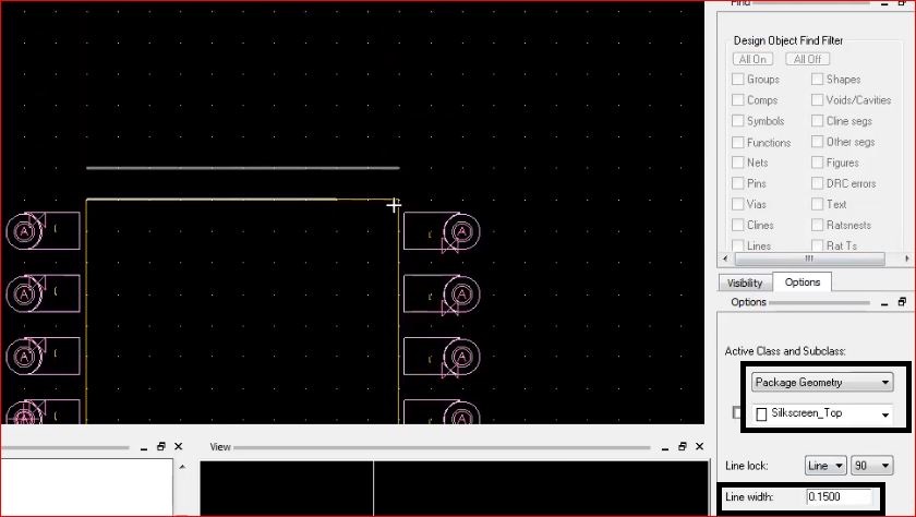
1. First you need to select Package Geometry under the active class and subclass section. Now, to draw the outer line of the pin, go to Add, and select Line.
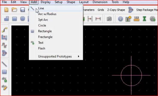
2. After creating the outline, go to Add, and select 3pt Arc, to draw the arc. According to the workspace scale (0.25 mm per unit), the diameter of this dummy pad is equal to 1.5 mm.
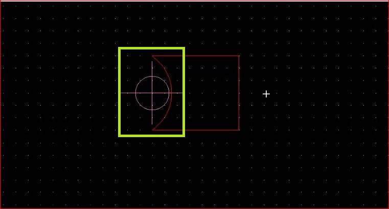
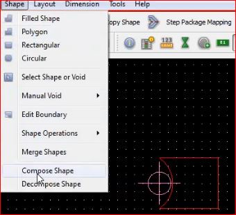
3. Now, go to Shape and select Compose Shape and click on the dummy pad to save the pad outline.
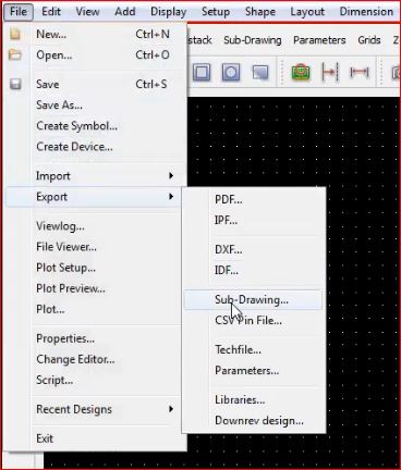
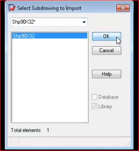
4. Next, go to File, Export, choose Sub-Drawing, and save the file with a designated name. Here the file is saved as shp90*32 and the type as a clipboard file.
5. Go to File, select Import, and choose the saved sub-drawing.
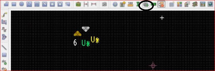
6. Now, you need to open the template that is saved in step 4. Go to file, open, and select the saved clipboard file(shp90*32). Next, click on the pad symbol on the toolbar to create a dummy pad.
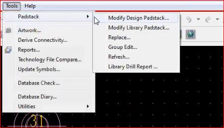
7. Go to Tools, click on Padstack and choose Modify Design padstack and place the pad.
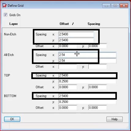
8. Select Grids from the Setup tab to modify the parameters.

9. Click on Copy to duplicate the created pads.
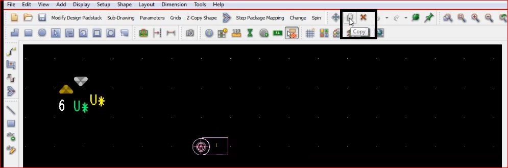
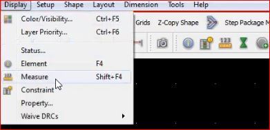
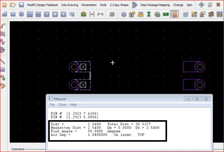
10. Now, click on Measure to check the pad dimensions.
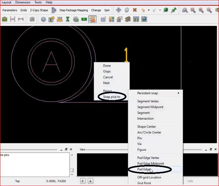
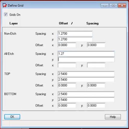
11. To modify the pad dimensions, right-click on the pad, select Snap pick to, and click on Pad edge. Now, select Setup and choose grid to define the spacing between the pads.
12. Now, you need to draw the assembly outline. Go to Package Geometry and select Assembly_top. To verify the pad spacing, click on measure.
13. Now add a silkscreen to the board with a line width of 0.15 mm. This option is available in Package Geometry.
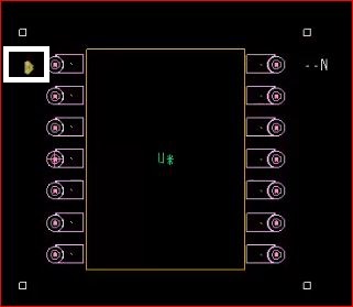
14. Designate the 1st pin using the pin indicator. Place it at a distance of 0.05 mm from the board edge.
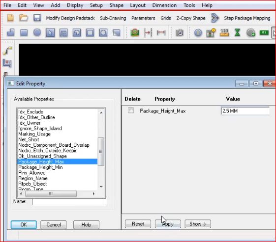
15. To define the board size, go to Edit, click on Package Height Max and set it to 2.5 mm. This depends on the your specifications.
16. Click on 3D from the toolbar to observe the model in 3-dimensional.
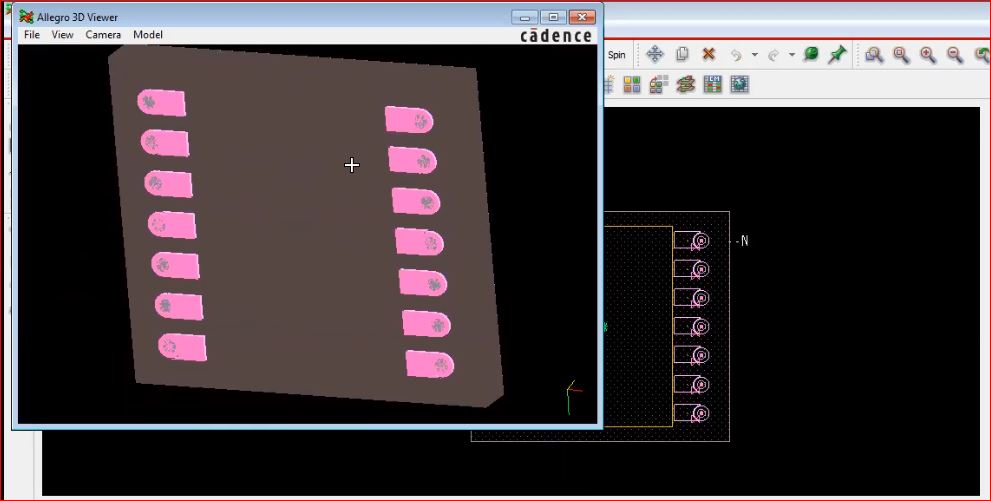
17. A castellated board with the given dimensions is created now.
How are castellated pins created on a PCB?
Castellated pins are manufactured by drilling plated-through holes on the edges of the board. After the drilling process, fabricators need to cut the holes into halves along the edge and attach a pad to it. These plated semi-holes can be used as soldering pads to attach the sub-assembly circuits to the main board. The process of creating these holes is also called edge plating or side plating.
Adhere to the following guidelines to establish a reliable board-to-board connection:
- Ensure no gaps between the two boards. Even a small gap will adversely affect the soldering process.
- When stacking boards, ensure that the thickness of the upper PCB is one-third the size of the lower one. This will aid in appropriate alignment and assembly.
- Castellated pins must match the SMD pads it is supporting.
Why should you choose a castellated holes PCB
Opting for a castellated circuit board can help you improve the efficiency of your design. A few of the advantages are listed below.
Quick and affordable assembly: Plated half-hole on the edges eliminate the use of board-to-board connectors. This fastens the board assembly process and reduces the overall cost.
Efficient thermal management: Complex systems such as aerospace and telecommunication devices feature high-temperature components, which increase the overall temperature of the board. Castellated circuit boards offer better heat dissipation when compared to other PCBs.
Improved signal integrity: The metallization of the edges prevents EMI on the inner layers and reduces the risk of electrostatic damage.
Acts as breakout boards: Castellated PCBs can be used as breakout boards for a specific area of a larger PCB. This facilitates the prototyping of integrated circuits and experimentation.

Signal Integrity eBook
6 Chapters - 53 Pages - 60 Minute ReadWhat's Inside:
- Impedance discontinuities
- Crosstalk
- Reflections, ringing, overshoot and undershoot
- Via stubs
Download Now
Design guidelines for castellated circuit boards
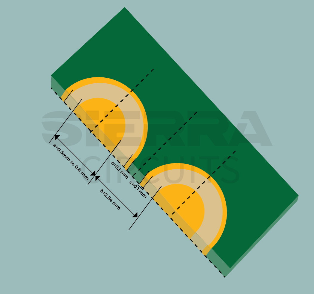
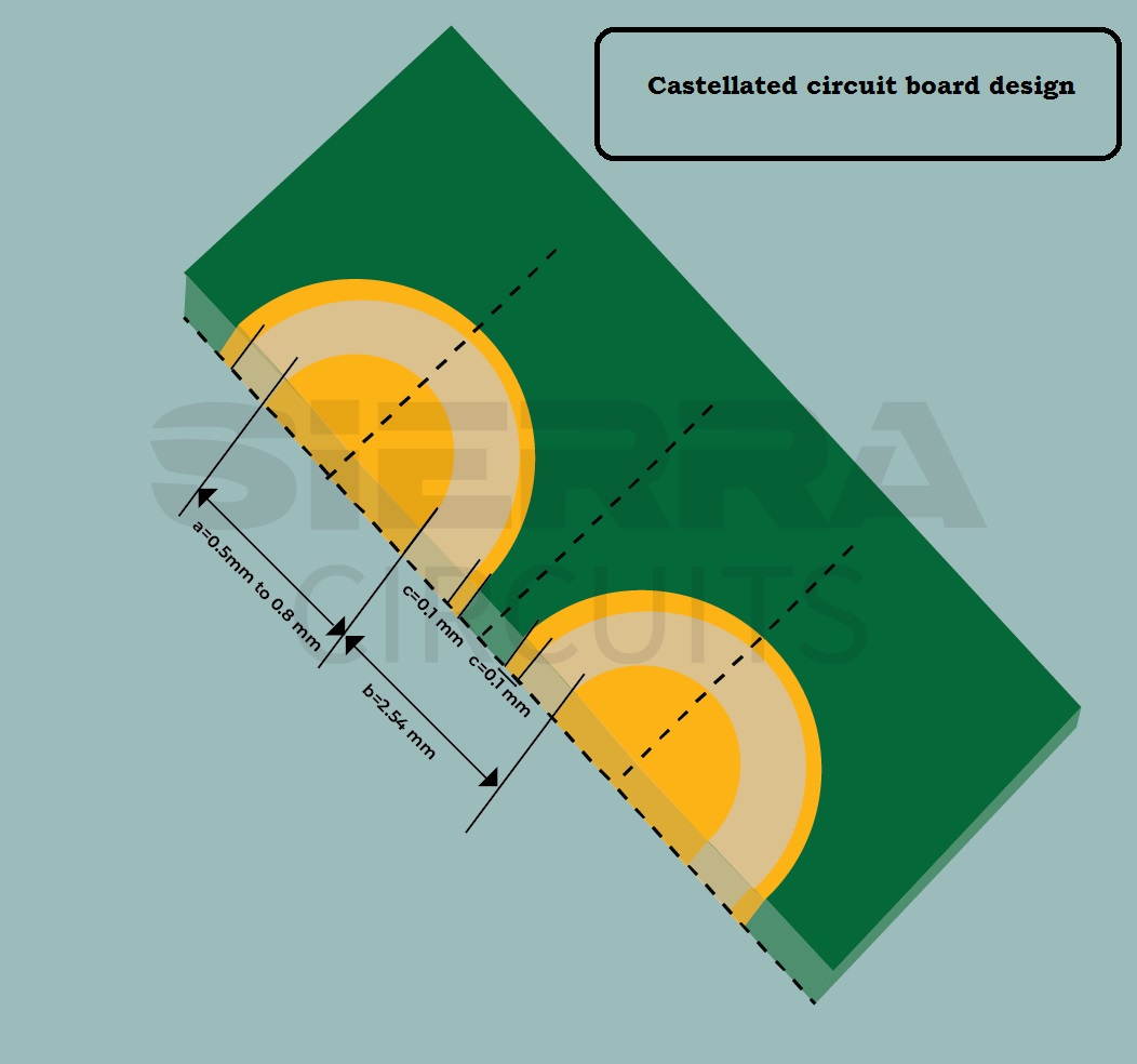
- Place the exact center of each castellated hole on the edge of your board. These holes must be plated through. Include them in the drill files.
- Always place the castellated holes on the top or bottom edges.
- Use pads for copper layers.
- Make sure you provide an accurate solder mask opening. This will prevent your board from corrosion and physical damage.
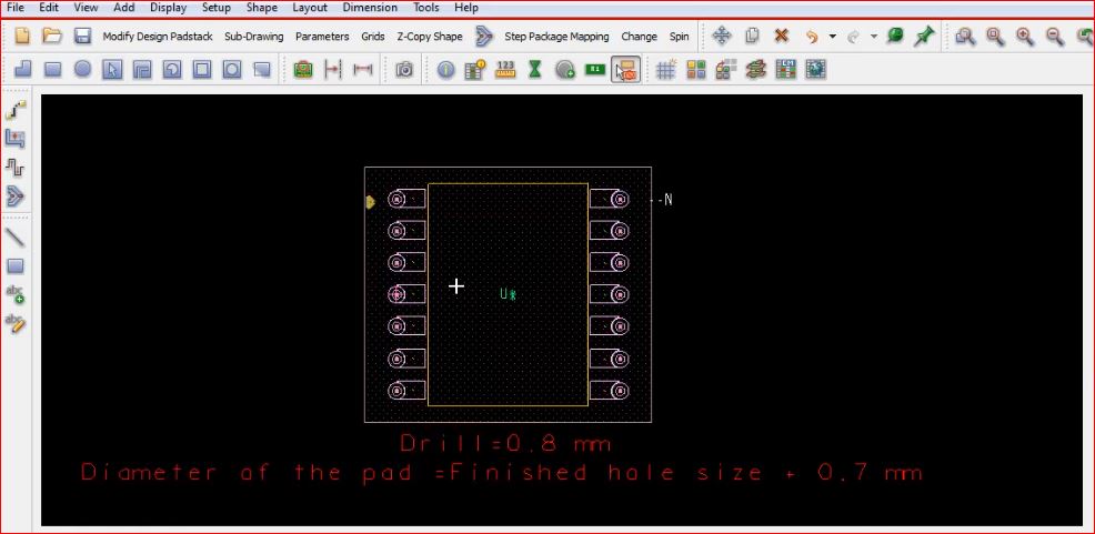
- Maintain the finished hole size [(a) shown in the image above] between 0.5 mm and 0.8 mm.
- Design the size of the castellated pads as per below:
- Diameter of the pad = Finished hole size + 0.7 mm
For example, if the finished hole size is 0.8 mm, then the pad diameter will be 1.5 mm. - Maintain sufficient width for the annular ring, or else the plating will break out.
- The minimum diameter for drilling half-holes is 0.5 mm.
- You can have a minimum solder mask clearance (c) of 0.1 mm.
- Keep the solder mask bridge between 0.1 mm – 0.15 mm.
- Keep the pads at a distance of 2.54 mm (b) from each other.
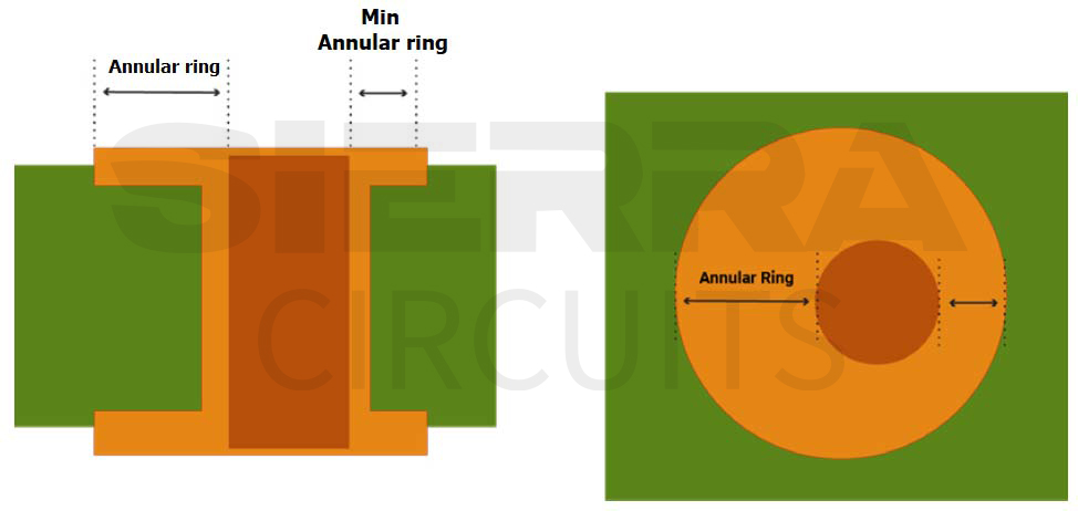
- Ensure the annular ring width is 0.3 mm per side. This is calculated as follows:
- Annular width = (Diameter of the pad-diameter of the finished hole) /2
- Diameter of the pad = Finished hole size + 0.7 mm
Need help in designing reliable PCBs? Our engineering team can help you with thermal management, stack-up design, and DFM analysis.
You can book a meeting with our experts or call us at +1 (800) 763-7503.

Edge plating: A technique to metalize castellated holes
Edge plating is a method used for the metallization of castellated pins. Here, copper will be deposited along the semi-hole walls. Follow these guidelines to ensure manufacturability.
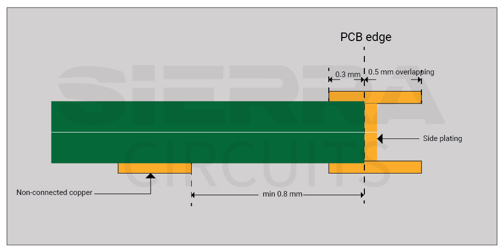
- Overlap from the board edge should be at least 0.5 mm.
- A minimum of 0.3 mm of connected copper must be defined on the connected layer.
- The spacing between the hole wall and the copper feature on a non-connected outer layer should be a minimum of 0.8 mm.
Why ENIG is preferred for edge plating
The surface finish options for castellated holes include ENIG, ENEPIG, HASL, and others. ENIG coating is preferred as it provides a smooth finish and eliminates the formation of lumps during the coating process.
Tolerances of castellation holes
IPC – 6012 defines the tolerances for castellation holes. The values are given in the table below.
| Parameters | Tolerances |
| Size of the pad | ± 20 % |
| Castellated hole size | ± 3 mils |
| Board thickness | 10% or ± 3 mils whichever is larger (thickness should be greater than or equal to 31 mils) |
| Drill diameter | ± 3 mils |
| Drill to copper | Minimum 8 mils |
| Hole to hole | 6 mils |
Castellation is a convenient and efficient way to establish board-to-board connections. It allows you to solder a sub-circuit directly to the main module eliminating the need for external connector pins. This significantly reduces the overall cost of the board and also speeds up the assembly process. We hope this tutorial was helpful in designing castellated boards using Altium Designer and Allegro. If you need any assistance in designing castellated PCBs, let us know in the comments section. We will be happy to help you.

Design for Manufacturing Handbook
11 Chapters - 96 Pages - 90 Minute ReadWhat's Inside:
- Annular rings: avoid drill breakouts
- Vias: optimize your design
- Trace width and space: follow the best practices
- Solder mask and silkscreen: get the must-knows
Download Now


