What is a schematic diagram?
A schematic diagram is a fundamental two-dimensional circuit representation showing the connectivity between different electrical components in a circuit board. Each of these components has its own footprint that defines the terminal geometry of the component. Schematics can be an extremely valuable troubleshooting tool as they trace out the connections in the circuit.
Sierra Circuits’ engineers and technicians have the experience to bring your PCBs to life.
How do you draw a PCB schematic?
Circuit diagrams were once drawn on paper by designers. Now, we have PCB design tools such as Altium, Allegro, Pads, Kicad, Tinycad, Express PCB, and others. These design tools constantly monitor logical and connection problems to ensure that the schematic designs are error-free. To make the circuit machine-readable, designers must follow the standard schematic design rules discussed below.

KiCad Design Guide
10 Chapters - 161 Pages - 180 Minute ReadWhat's Inside:
- Creating a component symbol library
- Setting up board parameters and rules
- How to route differential pairs
- How to place of components
Download Now
Schematic design rules to follow
Page size
The majority of design tools include a variety of page sizes such as A1, A2, A3, and so on. In most cases, the tools will choose A4 as the default page size. Select the size based on the size of your circuit design.
Page naming convention
The schematic’s logical blocks should be separated by pages. The letters A, B, C, and so on can be used to label the pages. This allows you to arrange the pages in alphabetical order. An example of such a naming convention is shown below.
- A_Block diagram
- B_Power supply
- C_ MCU interface
- D_Memory interface
- E_ Revision history
Symbol creation
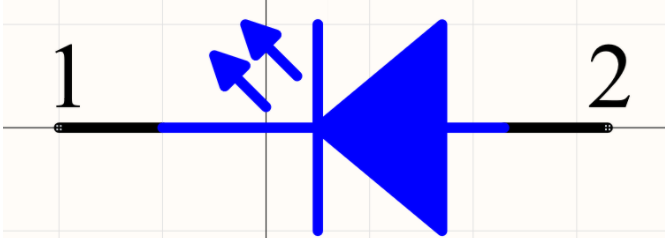
Symbols should always be created such that the pins are placed on the grids as shown in the image above. Grids help you to reference the parts properly and make the required connections.
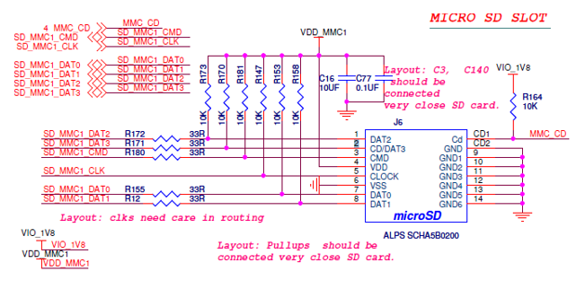
Notes/comments/revision history
Provide all the required notes related to the schematic. Notes can either be written on independent pages or on schematic pages. Jumper status, PCB layout constraints/guidelines are examples of notes. The image below shows a schematic page with notes written on it.
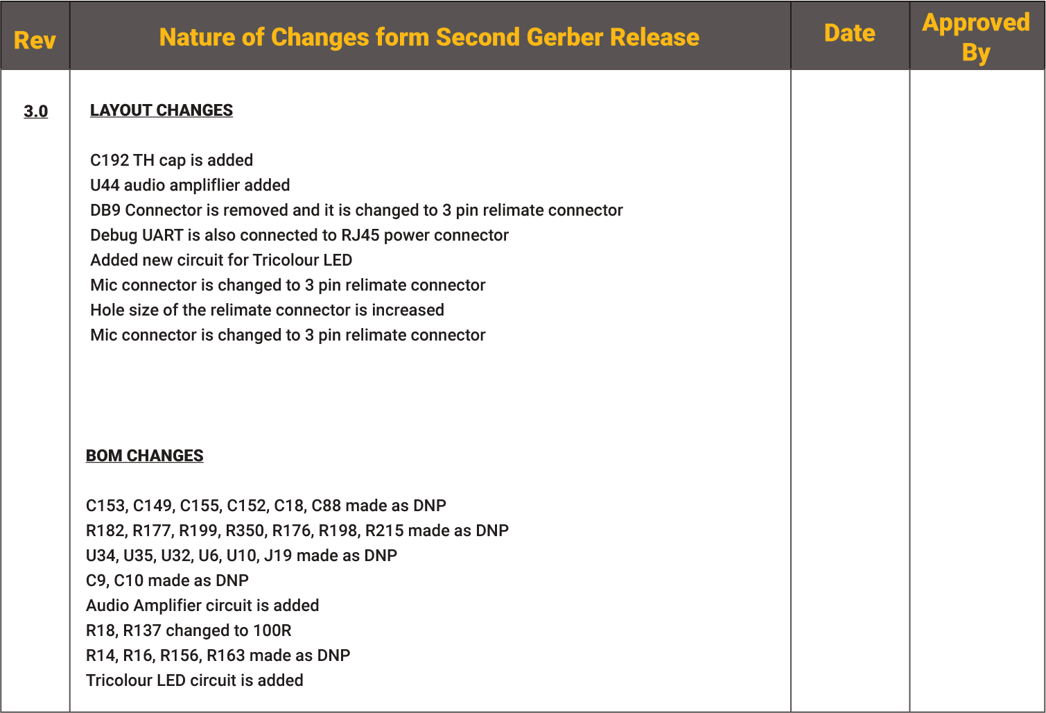
The modifications to the design are recorded in the revision history. This document contains information such as the date and description of the changes made, the authors’ and reviewers’ names. The revision history is usually found on the first or last page. Below is an example of a schematic revision history.
To learn more about PCB schematic, read How to Draw and Design a PCB Schematic?
Beat competitors to the market. Reduce Respins with our Zero-Defect Guarantee.
With Turnkey PRO, Sierra Circuits delivers full turnkey PCB assemblies guaranteed to work.
What is the difference between schematic and layout?
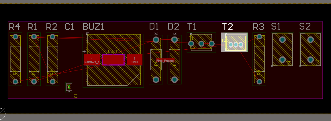
A schematic contains a netlist, which is a simple data structure that lists every connection in the design, as specified in the drawing. In contrast, the PCB layout is an electronic replica of the board, which shows within a well-defined area/boundary the exact physical locations of every component on the circuit board and shows the physical wires (traces) that connect them together.
Rules to draw a schematic
To achieve successful schematic design, follow the rules below:
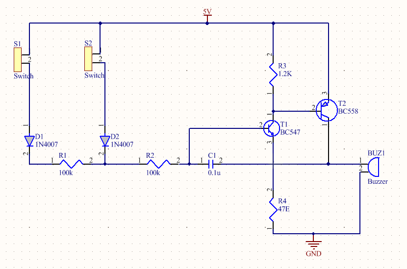
- Electrical connections between the components are represented by lines. Lines that intersect with each other are not connected unless there is a node present at the point of intersection.
- It is always a good practice to have only 3 lines connected to a node.
- In complex circuits, it is recommended to assign names to nets. The nets with the same name are assumed to be connected.
- The pin numbers, polarity, values, and net names should be written horizontally.
- Place the inputs on the left and outputs on the right.
- Design schematic sections in functional blocks.
- Always place pin numbers on the outside of the symbol graphic.
- Sheet connection symbols should always be placed on the extreme left edge or extreme right edge of the page.
- Place the title block on the lower right corner of the first sheet. The title block should display the following information:
- Title
- Part number
- Revision (if any)
- It is a good practice to have a page showing the block diagram of the circuit and also a history page that lists the changes in the schematic over a period of time.
Try our free Better DFM tool and save time and money. Our automated platform will catch any PCB design error ahead of time and prevent on-holds and re-spins.
Get started by uploading your Gerber files here.


