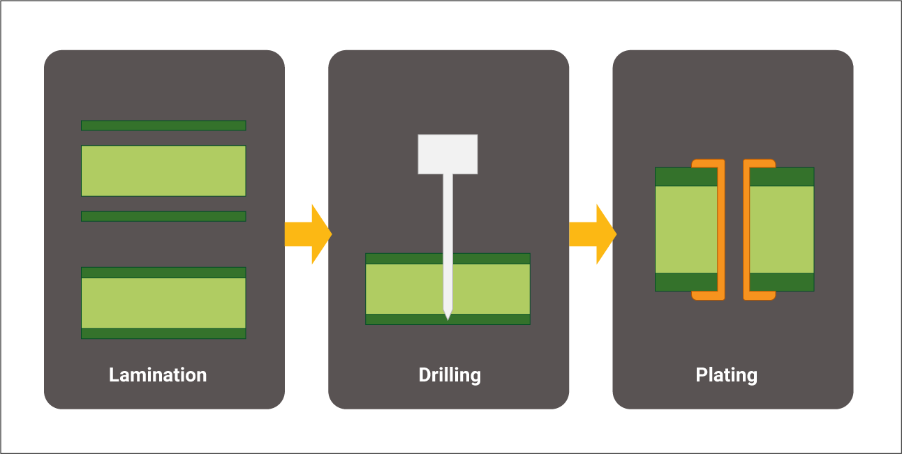
Drilling and through-hole plating are two crucial processes during PCB manufacturing. Drilling lays the foundation for creating holes or slots on the circuit board. These drilled structures are used for securing components and/or interconnecting layers. To establish electrical connections, the drilled structures must be plated. This process of plating the entire structure using copper for conductivity is called through-plating (via plating).
Drilling starts once the lamination is completed and is followed by the hole plating. The flowchart representing the order is given below:
PCB drilling
PCB drilling forms the basis for vias and inter-layer connectivity. Even though it is a commonly used process all around the world, when it comes to circuit boards, drilling is very expensive. This process should be carried out with utmost precision since once a hole is drilled, it cannot be reversed. Hence drilling becomes a time-consuming affair during manufacturing.
Drilling speed
Mechanical holes can be drilled at a speed of 5000 holes per hour. With the increase in the number of holes, the overall cost of the circuit boards increases. Also, as the holes get closer to each other, care should be taken so that they maintain the minimum drill-to-drill spacing.
Beat competitors to the market. Reduce Respins with our Zero-Defect Guarantee.
With Turnkey PRO, Sierra Circuits delivers full turnkey PCB assemblies guaranteed to work.
What is used to drill holes in circuit boards?
To drill PCBs, we have two technologies: mechanical and laser.
Mechanical drilling
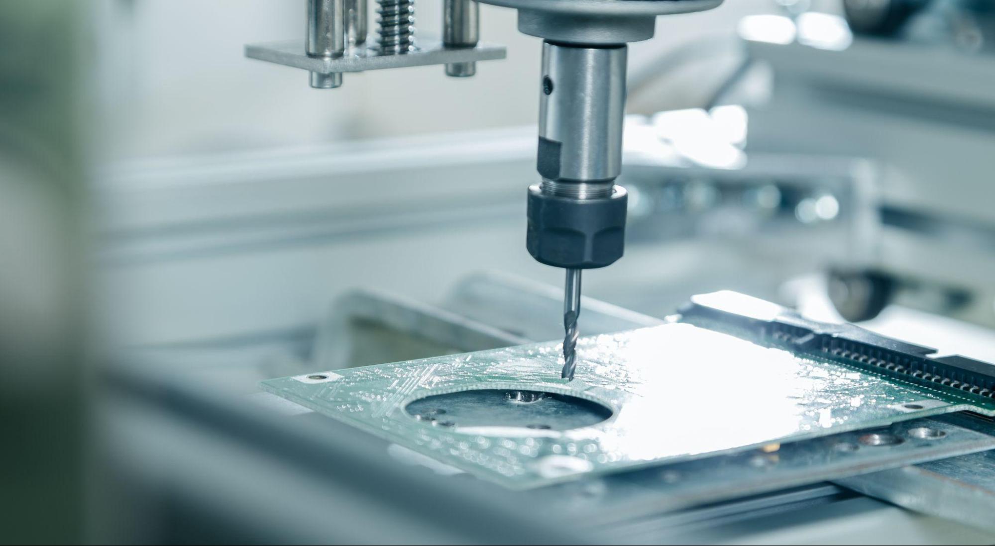
Mechanical drilling is used to create through-holes. It is also used for back drilling. In this technology, drill bits are used and the smallest hole can be drilled with a diameter of about 6mils.
Laser drilling
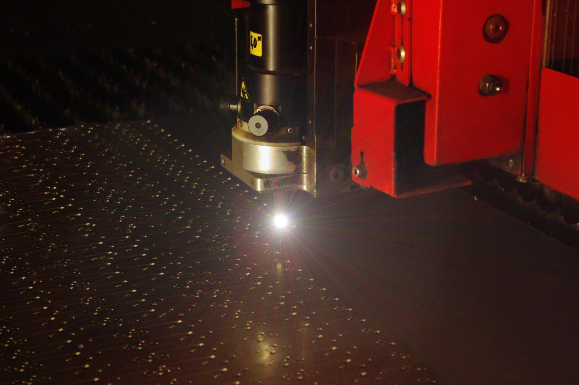
For more precise drills, laser drilling is used. This technology enables drilling holes that are smaller than those drilled mechanically. This process takes place with no contact between the board and the tool. Usually, it comes in handy when holes are drilled between layers of the circuit board. When a through-hole is required, this technique is seldom implemented.
Laser drilling is more frequently employed for the creating blind and buried vias. The minimum diameter of the hole obtained using this technique is 4mils.
Drill tolerances
| Feature | Tolerance |
| Drill tolerance for PTH | ±3 mils |
| Drill tolerance for NPTH | ±2 mils |
| Via location | 1 mil |
Important aspects of drilling
The process of drilling is not just about the size of the holes to be created, but also involves many aspects whose design determines the overall efficiency of the process. Below are the important ones.
Aspect ratio
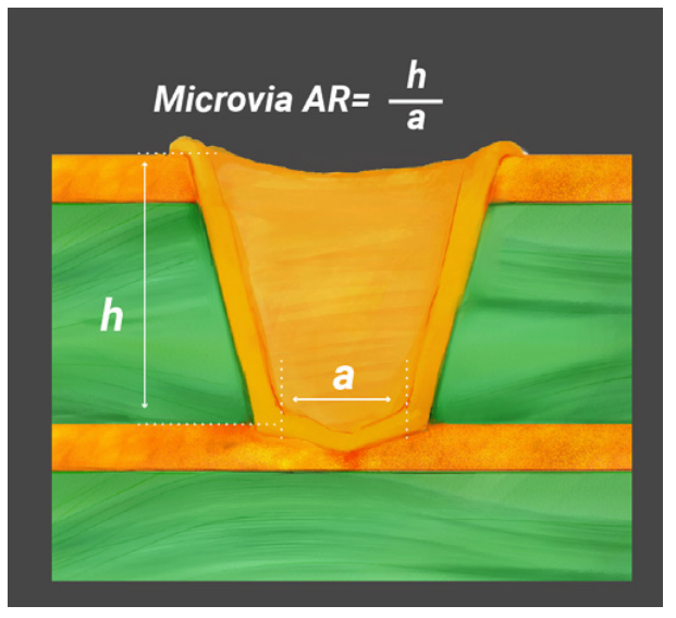
The aspect ratio (AR) for a through-hole is defined as the ratio between PCB thickness and the diameter of the drilled hole. The thickness/depth of the microvias is not the same as that of the board. Hence for microvias, the aspect ratio is defined as the ratio between the depth of the ]hole and its diameter.
For through-holes, the ideal aspect ratio is 10:1 and for microvias, it is 0.75:1.
AR is an important factor that determines the ease with which copper plating can be done inside the holes. When the depth of the hole increases and the diameter decreases (higher aspect ratio), it is difficult to copper plate the hole.

IPC Class 3 Design Guide
8 Chapters - 23 Pages - 35 Minute ReadWhat's Inside:
- IPC guidelines for manufacturing defects
- IPC standards for assembly processes
- Common differences between the classes
- IPC documents to set the level of acceptance criteria
Download Now
Annular ring and drill-to-copper
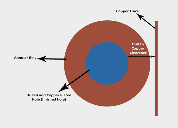
Annular ring is the area of a copper pad that surrounds a drilled hole. It helps to establish connections between a plated hole and nearby traces or other copper structures.
The drill to copper is the land clearance between the edge of a drilled hole to the nearest copper feature.
The finished hole to copper clearance will be the drill to copper clearance along with the copper plating thickness. Finished hole to copper clearance = drill to copper clearance + plating thickness x 2.
If the drill diameter is 6 mil and the plating thickness is 1 mil, then: finished hole to copper clearance = 6 + 1 x 2 = 8 mil.
For drill to copper, always drilled hole edge is considered.
The annular ring requirements for mechanically drilled blind, buried, and through-holes on ½ oz copper is given in the tables below. These values should be maintained for class 2 or class 3 acceptance.
| Drill and pad diameter IPC class 2 (for ½ oz copper) | ||||
| Drill | Pad | Anti-pad | PCB thickness | Aspect ratio |
| 0.006” | 0.016” | 0.026” | Up to 0.039” | 6.05:1 |
| 0.008” | 0.018” | 0.028” | Up to 0.062” | 7.75:1 |
| 0.010” | 0.020” | 0.03” | Up to 0.100” | 10:01 |
| 0.012” | 0.022” | 0.032” | Up to 0.120” | 10:01 |
| 0.0135” | 0.024” | 0.034” | Up to 0.135” | 10:01 |
| Drill and pad diameter IPC class 3 for ½ oz copper | ||||
| Drill | Pad | Anti-pad | PCB thickness | Aspect ratio |
| 0.008” | 0.023” | 0.033” | Up to 0.062” | 7.75:1 |
| 0.010” | 0.025” | 0.035” | Up to 0.100” | 10:01 |
| 0.012” | 0.027” | 0.037” | Up to 0.120” | 10:01 |
| 0.01325” | 0.028” | 0.038” | Up to 0.135” | 10:01 |
Now for values other than ½ oz copper, these parameters are as given in the tables below.
| Drill and pad diameter IPC class 2 | ||
| Pad diameter over the drill | ||
| < 8 layers | > 8 layers | |
| ¼ oz copper | 0.010” | 0.010” |
| ⅜ oz copper | 0.010” | 0.010” |
| ½ oz copper | 0.010” | 0.010” |
| 1 oz copper | 0.012” | 0.012” |
| 2 oz copper | 0.014” | 0.014” |
| 3 oz copper | 0.016” | 0.016” |
| 4 oz copper | 0.018” | 0.018” |
| Drill and pad diameter IPC class 3 | ||
| Pad diameter over the drill | ||
| < 8 layers | > 8 layers | |
| ¼ oz copper | 0.010” | 0.010” |
| ⅜ oz copper | 0.010” | 0.010” |
| ½ oz copper | 0.010” | 0.010” |
| 1 oz copper | 0.012” | 0.012” |
| 2 oz copper | 0.014” | 0.014” |
| 3 oz copper | 0.016” | 0.016” |
| 4 oz copper | 0.018” | 0.018” |
| Drill and pad diameter IPC class 3a | ||
| Pad diameter over drill | ||
| < 8 layers | > 8 layers | |
| ¼ oz copper | 0.010” | 0.010” |
| ⅜ oz copper | 0.010” | 0.010” |
| ½ oz copper | 0.010” | 0.010” |
| 1 oz copper | 0.012” | 0.012” |
| 2 oz copper | 0.014” | 0.014” |
| 3 oz copper | 0.016” | 0.016” |
| 4 oz copper | 0.018” | 0.018” |
Sierra Circuits’ engineers and technicians have the experience to bring your PCBs to life.
Start building your quote online now.
What is the difference between a plated through-hole and a non-plated one?
Holes/vias are divided into plated through-holes (PTH) and non-plated through-holes (NPTH). PTHs are conductive holes used for electrical interconnection because of their copper plating. NPTHs are non-conductive holes used for holding the components in position.
What is through-hole plating?
A through-hole is a hole that begins at the top layer and spans the entire depth of the circuit board and ends in the bottom layer. The process of plating a through-hole with copper to make it conductive is called through-plating. NPTH does not require plating since they are not supposed to have electrical conduction.
We follow a general thickness of 0.0008″ to 0.0012″ (20 microns to 30 microns) for through-plating. The maximum hole size allowed for plated holes is 246 mils.
How are PCBs plated?
There are two methods of plating: electroless copper plating and electroplating.
Electroless copper plating
The through-plating process usually happens through electroless copper plating. Using this method, an even layer of copper is deposited on the required area. First, the bare boards go through a series of baths for cleaning. Then the areas that need to be coated are covered with a catalyst like Palladium. Then these areas are dipped in a bath with copper salts and reducing agents like formaldehyde. This will lead to the deposition of copper inside the hole region.
Copper plating the interior part of the holes becomes a tedious task when the diameter is decreased and the depth of the hole is increased (high aspect ratio). In this case, a copper plating bath of high throwing power would be required to make the solution go into the tiny deep holes and deposit copper in them.
Electroplating
The electroplating method uses an anode, cathode, and electrolyte. This process requires electricity to initiate the conduction and, thus, the plating. This method is generally used for plating the surfaces of PCBs and not for holes.
Drills and through-plating require a lot of care and precision. These expensive processes determine the overall cost and efficiency of a PCB.
The plating quality does not directly impact the aspect ratio and pad diameter. These parameters are primarily influenced by the structural design and layout of the circuit.
Try our free Better DFM tool and save time and money. Our automated platform will catch any PCB design error ahead of time and prevent on-holds and re-spins.
Get started by uploading your Gerber files here.


