


Contents

On-demand webinar
How Good is My Shield? An Introduction to Transfer Impedance and Shielding Effectiveness
by Karen Burnham
Designing PCBs for AI servers and hyperscale data center platforms requires architectures that support extreme routing density, high-speed serializer/deserializer (SerDes) signaling, and low impedance power delivery.
Layout engineers and signal integrity experts must adopt HDI for fine-pitch BGAs and select materials that meet the loss budgets of 112G and emerging 224G PAM4 signaling for high-performance computing systems.
In this article, you’ll learn printed board types used in hyperscale facilities, how to pick materials for 112G/224G signaling, and stack-up and layout techniques for long-term reliability.
Highlights:
- Use HDI in data center PCBs when BGA pitch ≤0.5 mm or the routing density exceeds the through-hole breakout capability.
- Design graphics processing unit (GPU) power delivery using multi-phase voltage regulators, low-inductance vias, and strong decoupling to handle sudden high current demands.
- Select very-low-loss or ultra-low-loss laminates (Df ≤0.004) for 112G/224G PAM4 channels, and reserve modified FR4 for non-critical layers.
- Use low-profile copper to minimize insertion loss at multi-GHz frequencies.
Data center hierarchical model
Modern servers deploy thousands of systems organized into racks and clusters. Each rack typically contains multiple high-performance processors connected through high-speed switch fabrics.
This infrastructure follows a hierarchical model, progressing from the facility level to clusters, racks, server nodes, and ultimately their underlying circuit boards.

Inside each server node, multiple boards work together to support compute, networking, storage, and power delivery functions. These subsystems are discussed in detail in later sections.
This model is widely deployed across major data center campuses in the United States, including Ashburn (Northern Virginia), Santa Clara (Silicon Valley), Dallas, Phoenix, and Atlanta.
Additional hyperscale campuses supporting global cloud and AI infrastructure are located in Quincy, Prineville, and Council Bluffs. These sites host massive server clusters operated by cloud providers such as Microsoft, Google, and Meta.
Amazon Web Services operates large campuses in Northern Virginia, Oregon, and Ohio.
Thousands of high-performance systems and network switches run continuously to support global cloud platforms and large-scale AI workloads.
What are the main challenges in high-speed boards for servers?
Higher network bandwidth requires faster SerDes signaling, which tightens board design margins and places stringent demands on signal integrity, materials, and manufacturing.
Modern systems operate at 112G and emerging 224G SerDes, where each lane carries 112 Gb/s and 224 Gb/s of data, respectively, using PAM4 modulation.
As networks evolve to support AI clusters and large-scale cloud workloads, each new Ethernet generation increases switch throughput while pushing signaling speeds higher. This is summarized in the table below.
| Ethernet generation | Switch port speed | Typical SerDes signaling |
|---|---|---|
| 100G Ethernet | 100 Gb/s | 25G NRZ |
| 400G Ethernet | 400 Gb/s | 56G PAM4 |
| 800G Ethernet | 800 Gb/s | 112G PAM4 |
| 1.6T Ethernet | 1.6 Tb/s | 224G PAM4 (emerging) |
These higher data rates introduce several key challenges in maintaining signal integrity, material performance, and manufacturing feasibility.
- Signal integrity constraints at 112G/224G data rates: At these speeds, circuit board channels are highly sensitive to loss and discontinuities. Factors such as dielectric loss, copper surface roughness, and via stubs significantly degrade signal quality and reduce channel margin.

Signal attenuation increases with increasing frequencies. The above graph illustrates total loss, skin effect loss, and dielectric loss.
Maintaining signal integrity, therefore, requires controlled impedance routing, minimized discontinuities, and optimized via structures.
- Material and stack-up limitations at multi-GHz frequencies: At high frequencies, board material properties become a dominant factor in channel performance. Standard FR4 materials are often too lossy, requiring the use of very-low-loss or ultra-low-loss laminates for high-speed layers.
Designers must also carefully engineer stack-ups to balance signal integrity, power delivery, and manufacturability, often using hybrid material strategies to control cost.
- Manufacturing challenges in high-speed, high-density boards: Higher electrical performance requirements in hyperscale boards push the limits of fabrication. Important constraints include microvia aspect ratio limits (typically 0.8:1), the need for multiple sequential lamination cycles in HDI designs, the use of very-low-profile copper to reduce loss, and tight back-drilling tolerances to eliminate via stubs.
To address these constraints, designs should prioritize manufacturing simplicity by using the least complex HDI structure that meets routing and signal integrity requirements. Close collaboration with fabrication partners is essential to ensure manufacturability.
Sierra Circuits utilizes self-learning automated scaling software (XACT) to ensure precision in HDI stack-up design. The system analyzes material type, thickness, and copper weight on each layer to accurately predict and compensate for material shrinkage.
Visit HDI PCB capabilities to learn more.
What are the commonly used PCBs in data center infrastructure?
Data center systems are organized into compute and accelerator trays that integrate multiple boards. These include server motherboards, network switch boards, storage controllers, backplanes, and power distribution boards, each optimized for compute, connectivity, storage, or power delivery functions.

| PCB modules | Primary function | Typical layer count | PCB technologies | Interface types | Material requirements |
|---|---|---|---|---|---|
| AI server motherboards (with GPU accelerator) | Host CPUs, GPUs, memory subsystems, and accelerator interconnects | 24–40+ | HDI | High-speed SerDes | Low-loss or very-low-loss laminates |
| Network switch | Connect servers through high-speed switching fabrics and interface with network interface cards (NICs) | 24–36+ | HDI | Ultra-high-speed SerDes (112G/224G) | Ultra-low-loss materials for 112G/224G |
| Storage controller | Manage non-volatile memory express (NVMe), SSD storage arrays, and data access | 12–24 | Standard multilayer (HDI optional) | PCIe and NVMe | Low-loss FR4 class laminates |
| Backplanes/interconnect | Provide high-speed PCIe connections between the server and NVMe SSD modules | 18–30 | High-speed multilayer | Long-reach SerDes channels | Low-loss materials for long channels |
| Power distribution | Deliver power from rack power supplies to server and accelerator modules | 4–12 | Heavy copper | Power delivery (DC) | High-Tg FR4 |
These board types are discussed in detail in the following sections.
What is a GPU accelerator board?
It is a dedicated add-in card used in AI servers to provide high-performance compute acceleration.
In artificial intelligence systems, GPUs are typically installed on accelerator cards that plug into the server motherboard through high-speed PCB interfaces. Each accelerator card contains a dedicated board designed to support extremely high compute density, large memory bandwidth, and high current delivery.
A typical GPU accelerator board features:
- GPU processors: The primary compute device responsible for executing AI workloads. These devices are typically packaged in large BGA packages containing thousands of solder balls.
- Graphics double data rate (GDDR) or high-bandwidth memory (HBM): Memory devices positioned close to the GPU processor to provide extremely high data transfer rates.
- Power delivery circuits: Multi-phase voltage regulator modules (VRMs) that supply stable power to the GPU core and memory subsystems.
- High-speed communication interfaces: PCIe or proprietary interconnects that allow the GPU to communicate with CPUs, networking devices, and other accelerators.

PCIe lane structure used to connect two devices. - Thermal management components: Cooling systems such as heat sinks, vapor chambers, and airflow structures designed to dissipate large amounts of heat.

Heat sink integration for data center PCB thermal management.
GPU circuit boards integrate high-speed signals, high-current power delivery, and advanced circuit board thermal management in a compact form factor.
AI server boards vs. network switch PCBs
Server motherboards are optimized for compute density, high-bandwidth memory interfaces, and high-current power delivery, while switch boards are designed for ultra-high-speed SerDes signaling and channel loss control. These boards operate within the same hyperscale infrastructure, but their printed board design priorities differ significantly.
The table below summarizes the key design differences between the two platforms.
| Design aspect | AI server/GPU boards | High-speed switchboards |
|---|---|---|
| Primary function | High-performance compute and AI acceleration | High-speed packet switching and network routing |
| Key components | GPUs, CPUs, HBM/DDR memory, accelerator interconnects | Switching ASICs, optical modules, SerDes interfaces |
| Main design challenge | Power delivery and thermal management | Channel loss and signal integrity |
| Typical signaling | PCIe, memory buses, accelerator interconnects | 56G/112G/224G PAM4 SerDes |
| Layer count | 24 to 40 (40+ in advanced server platforms) | 24 to 36 (40+ for 112G/224G switch ASIC platforms) |
| Design focus | PDN stability, dense BGA routing | Loss control, impedance continuity |
Although both platforms often require HDI stack-ups and low-loss materials, AI server boards are primarily constrained by power density and memory routing, while switch boards are constrained by signal integrity across long high-speed channels.
For high-density layout strategies, download the HDI PCB Design Guide.

HDI PCB Design Guide
5 Chapters - 52 Pages - 60 Minute ReadWhat's Inside:
- Planning your stack-up and microvia structure
- Choosing the right materials
- Signal integrity and controlled impedance in HDI
- Manufacturing considerations for higher yields
Download Now
What are storage controller boards and NVMe backplane boards?
In data centers, dedicated control boards manage data flow between host processors and storage devices, while backplane boards provide the physical interconnect that links multiple SSDs to the server via PCIe.
Storage systems in hyperscale data centers rely on NVMe backplanes and storage controller boards to connect processors with large arrays of SSDs. These boards route multiple PCIe lanes between host processors, storage controllers, and drive connectors, enabling high-throughput data access across storage clusters.
Unlike GPU accelerator boards that are dominated by compute and power delivery constraints, storage boards are primarily limited by PCIe signal integrity and high connector density. Maintaining reliable PCIe communication across multiple connectors and long routing paths requires careful impedance control and stack-up planning.
| Design aspect | Storage controller board | NVMe backplane |
|---|---|---|
| Primary function | Interface CPUs with storage; manage and switch PCIe traffic | Physically connect large numbers of SSDs to the system |
| Typical signaling | PCIe Gen4/Gen5 (sometimes Gen6 emerging) | PCIe Gen4/Gen5 differential pairs |
| Main components | PCIe switch ASICs, storage controllers, clocking ICs | High-density SSD connectors |
| Layer count | ~12–22 layers (24+ with dense PCIe ASICs) | ~18–30 layers (driven by connector density and PCIe routing complexity ) |
| Connector density | Moderate to high (board-to-board, cable connectors) | Extremely high (U.2/U.3 and EDSFF SSD connectors) |
| Design focus | High-speed PCB routing, power integrity, and application-specific integrated circuit (ASIC) breakout | Differential impedance control, connector transitions |
Since PCIe channels often traverse multiple connectors and extended printed board traces, you must carefully control impedance, skew, and insertion loss to ensure reliable high-speed data transfer across the storage backplane.
To learn how to integrate connectors to your high-speed designs, watch our webinar: high-speed success at 28-56-112 Gbps with connector-PCB integration.
How to select materials for hyperscale server boards?
Different laminates are assigned to specific layers based on signal speed and performance requirements. This approach allows you to reserve high-performance materials for critical channels while controlling overall manufacturing cost.
As hyperscale data center networks transition to 112G and emerging 224G PAM4 signaling, material selection becomes a vital factor in maintaining channel performance. At these data rates, insertion loss caused by dielectric absorption and copper surface roughness can significantly reduce signal margin across high-speed links.
In many server platforms, hybrid stack-ups combine multiple material types within a single printed board for cost optimization. Critical high-speed (112G or 224G SerDes) layers may use very-low-loss or ultra-low-loss laminates, while other layers use modified FR4 materials for cost efficiency.
| Material category | Typical use | Characteristics |
|---|---|---|
| Standard FR4 | Power, control, and low-speed digital layers | Too lossy for 112G SerDes channels |
| Modified low-loss FR4 | Mainstream AI server boards | Typical Dk ≈ 3.6–3.8, Df ≈ 0.005–0.009 |
| Very-low-loss laminates | High-speed SerDes layers | Used for 112G PAM4 channels |
| Hybrid stack-ups | Critical long-reach channels | Combines FR4 layers with low-loss or ultra-loss laminates |
| PTFE | RF or microwave signal paths, extreme low-loss requirements | Lowest loss (Df≈ 0.0002-0.001, Dk ≈ 2.1-3.0); used selectively in high-end hybrid stack-ups; costly and hard to fabricate |
When selecting materials for high-speed server boards, designers should also consider additional physical properties such as:
- Stable dielectric constant (Dk): Target Dk in the range of ~3.0-3.7 with minimal variation across frequency (ΔDk ≤±0.05–0.1 from 1 GHz to 10+ GHz) to maintain impedance stability.
- Low dissipation factor (Df): Use materials with Df ≤0.0025 to minimize dielectric loss in 112G/224G high-speed channels.
- High glass transition temperature (Tg): Select materials with Tg ≥170 °C (preferably 180-200°C+) to ensure thermal reliability under sustained workloads.

Glass transition temperature (Tg) of FR4. - Low Z-axis coefficient of thermal expansion (CTE):
- Below Tg: ≤50 ppm/°C
- Above Tg: ≤200–250 ppm/°C
This helps prevent via failure during thermal cycling.
- CAF resistance: Use CAF-resistant laminates to prevent conductive anodic filament failures in high-density multilayer boards. Common materials include Isola Astra MT77, Isola Tachyon 100G, Rogers RO3003, and Rogers RT/Duroid 5880.
Close coordination with the fabricator is essential to confirm laminate availability, thickness tolerances, and resin content before finalizing the stack-up.
At Sierra Circuits, we control curing parameters like temperature, pressure, and time to minimize stress and prevent layer misalignment in hybrid stack-ups.
To learn more, talk to a PCB expert: Book a meeting or call us at +1 (800) 763-7503.
How do circuit board materials affect signal loss in 112G and 224G channels?
Material properties such as dielectric loss, glass weave variation, and copper surface roughness directly impact high-speed channel margin. As signaling rates reach 112G and 224G PAM4, material behavior becomes a dominant factor in channel performance. At these speeds, signal loss is no longer determined solely by routing geometry.
Material selection for 112G and especially 224G systems is typically organized into performance tiers based on dielectric loss characteristics.
| Material category | Typical Df (10 GHz reference) | Application domain |
|---|---|---|
| Ultra-low loss (ULL) | ≤0.0020 | Long-reach 112G/224G SerDes channels |
| Very low-loss (VLL) | 0.0021–0.0040 | PCIe Gen6 and shorter 112G links |
| Low/mid-loss | 0.0050–0.0100 | Power, control, and low-speed layers |
Since ULL materials significantly increase circuit board cost, most server platforms use hybrid stack-ups, reserving these laminates for critical SerDes routing layers while using modified FR4 or VLL materials for the remainder of the stack.

Two critical physical attributes in high-speed channels
1. Glass weave skew: Printed board laminates use woven fiberglass cloth embedded in resin. Standard glass styles create alternating bundles of glass fibers and resin pockets, which exhibit different dielectric constants.
When high-speed differential pairs route over these non-uniform regions, one trace may propagate faster than the other, introducing intra-pair skew. At 112G and especially 224G PAM4 signaling rates, even small propagation differences can reduce eye margin.
Common mitigation techniques include:
- Pick spread-glass laminate styles such as 1067 or 1078. The spread glass creates a uniform dielectric environment and ensures consistent impedance.

106 and 1067 glass weave style. Image credit: Isola R&D Laboratories. - Select prepregs with higher resin content to reduce dielectric variation.
- Route differential pairs slightly off-angle relative to the glass weave to avoid propagation delays.
These techniques help reduce skew variation across long high-speed channels.
2. Copper surface roughness: At multi-GHz frequencies associated with 112G and 224G signaling, current flow is concentrated within the outer micron of the conductor due to the skin effect. Surface roughness increases the effective conductor path length, which increases insertion loss.
To reduce conductor loss, high-speed server boards typically use very-low-profile copper foils, including:
- Hyper very low profile (HVLP) copper
- Very low profile, second-generation (VLP2) or equivalent copper foils

As copper roughness strongly affects high-frequency loss, its parameters must be included in signal integrity simulations and channel modeling to accurately predict insertion loss and channel margin.
Careful control of dielectric loss, glass weave variation, and copper roughness is therefore essential for achieving reliable 224G PAM4 channel performance in next-generation data center platforms.
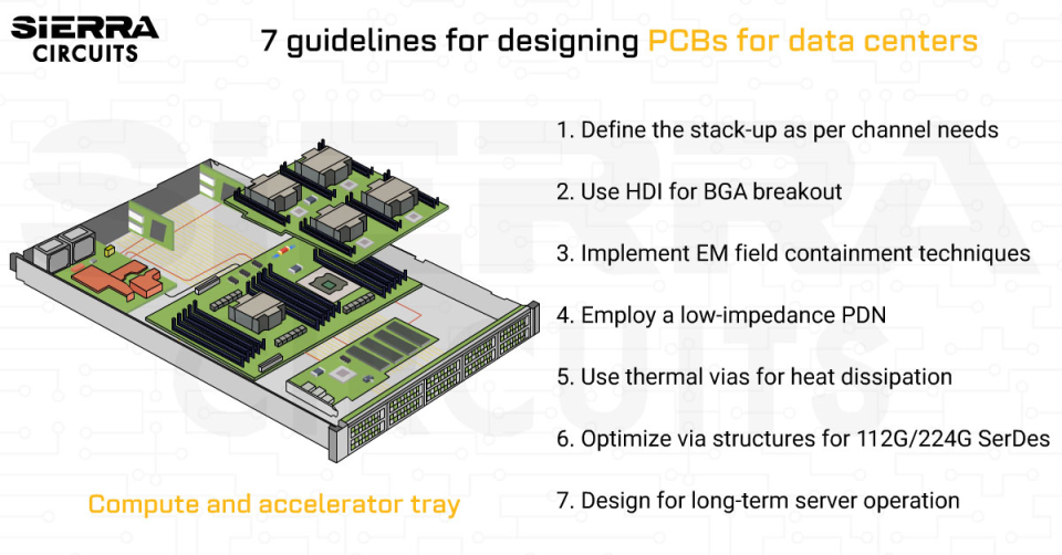
7 guidelines for designing PCBs for data centers
Modern server platforms integrate large BGA processors, high-speed SerDes channels, and high-current accelerators, all of which impose strict constraints on printed board build-up, routing topology, and component placement.
Follow these design practices to ensure stable electrical performance and long-term reliability in these environments.
1. Define the stack-up based on high-speed channel and PDN requirements
Layer stack architecture directly determines both channel loss behavior and power distribution network (PDN) impedance in hyperscale server boards. At 112G and 224G PAM4 data rates, stack-up planning should occur before schematic capture or routing begins.
Essential stack-up guidelines include:
- Position high-speed SerDes layers within tightly coupled reference plane pairs to control impedance and suppress mode conversion in multi-GHz channels.
- Pair power and ground planes to achieve low-inductance PDN structures capable of supporting large transient currents.
- Maintain symmetrical copper distribution to ensure dimensional stability in a high-layer-count (>20 layers) server board.
- Use inner layers for high-speed channels where shielding from external noise is strongest.
Utilize field solver tools to verify impedance targets such as 50 Ω single-ended and 100 Ω differential before finalizing dielectric thickness and trace geometries.
2. Use HDI for high-speed channel integration and BGA breakout
Modern server processors and GPU accelerators use large BGA packages with thousands of pins, making traditional through-hole breakout techniques insufficient for routing high-speed signals and dense power networks.
At 112G and emerging 224G PAM4 data rates, conventional multilayer structures cannot support the required channel density and via performance. HDI architectures become necessary when breakout density, high-speed channel requirements, or PDN via density exceed the capability of conventional multilayer circuit boards.
| Design condition | Standard multilayer | HDI |
|---|---|---|
| BGA pitch | ≥0.65 mm | ≤0.5 mm |
| Breakout density | 1–2 signal layers | ≥4 signal layers |
| Signaling speed | ≤10 Gbps | 56G/112G/224G PAM4 |
| Via strategy | Through-hole | stacked vias, blind/buried microvias, via-in-pad |
| Routing density | Standard differential pairs | Dense differential buses |
In GPU accelerator boards, HDI routing is often required to support HBM interfaces, which operate at extremely high data rates and require strict signal integrity control.
If via-in-pad or stacked microvias are required under the densest BGA regions, HDI becomes mandatory regardless of overall net count.
For more on breakout strategies, see:
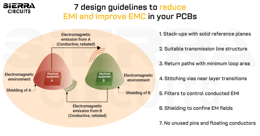
3. Implement effective electromagnetic containment techniques
High-bandwidth memory interfaces between the GPU and memory devices operate at extremely high data rates and are sensitive to impedance discontinuities, skew, and crosstalk.
To preserve signal integrity, designers should:
- Route memory channels on dedicated inner layers sandwiched between ground planes.
- Apply strict length matching and skew control across differential pairs to prevent lane-to-lane misalignment at 112G+ rates.
- Minimize GPU-to-memory interconnect length to reduce insertion loss and timing uncertainty.
- Add via stitching grids and ground fences around dense high-speed channel clusters to mitigate electromagnetic interference (EMI).

Via stitching to mitigate EMI. - Isolate high-current VRM regions from sensitive SerDes and memory interfaces to reduce noise coupling.
For more, download the EMI and EMC Design Guidelines for PCBs.
EMI and EMC Design Guidelines for PCBs
6 Chapters - 77 Pages - 75 Minute ReadWhat's Inside:
- How electromagnetic interference is generated and spreads
- How to identify EMC requirements and applicable standards
- How to design for electromagnetic resilience
- Common EMI sources: Switching circuits, PWM signals, and motors
- PCB structures that cause radiated emissions
- Practical layout, stack-up, filtering, and shielding guidelines
Download Now
4. Employ a low-impedance power distribution network
Modern GPU accelerators can consume hundreds of watts of power, generating rapid current transients during parallel workload execution. Maintaining stable voltage delivery, therefore, requires a carefully engineered PDN with low impedance across a wide frequency range.
Effective PDN design strategies include:
- Use multi-phase VRM architectures to support large transient currents from AI workloads.
- Utilize low-resistance power planes to maintain voltage stability under high GPU current densities.
- Employ low-inductance via networks to control PDN impedance at high frequencies.
- Distribute decoupling capacitors between the VRMs and GPU to control PDN impedance during transient load conditions.

Decoupling capacitors are distributed along the path from the VRM to the IC in data center PCBs.
In high-power accelerator boards, power planes often serve a dual role as thermal spreading layers, helping distribute heat away from the processor while maintaining low electrical impedance.
5. Use copper planes and thermal vias for heat spreading
High-power GPU devices generate significant heat, requiring efficient heat transfer through the printed board structure to prevent thermal hotspots.
Accelerator boards, therefore, incorporate several thermal management techniques:
- Use dense thermal via arrays beneath GPU packages to conduct heat through high-layer-count stack-ups.

A thermal via array is added under the component’s pad to increase the heat dissipation. - Leverage internal copper planes to spread heat across the circuit board and reduce thermal gradients in high-density regions.
- Align high-power components with system airflow paths to support effective cooling under sustained workloads.
6. Optimize via structures for 112G and 224G SerDes channels
In high-speed SerDes channels, via structures are a dominant source of signal integrity degradation. Poorly optimized vias can introduce impedance discontinuities and resonant stubs that significantly reduce channel eye margin at gigahertz frequencies.
Unused portions of through-hole vias act as resonant stubs, reflecting energy back into the transmission path and distorting high-speed signals.
To mitigate these effects, you should implement the following strategies:
- Specify back-drilling to remove unused via barrels, eliminating resonant stubs.
- Constrain stub lengths below approximately 10 mil, depending on channel frequency.
- Use microvias or blind/buried vias to eliminate stub formation in fine-pitch BGA breakouts (≤0.5 mm pitch).
- Validate drill depth tolerances to avoid DFM errors.
7. Design for reliability and long-term server operation
Hyperscale server infrastructure operates continuously for years under high electrical, thermal, and mechanical stress. Printed board materials, mechanical structures, and manufacturing processes must therefore support long-term reliability.
Design considerations include:
- Reinforce press-fit connector regions to withstand insertion forces.
- Add mechanical support beneath large heatsinks or heavy components.
Many hyperscale server platforms follow IPC-6012 class 2 benchmarks, while accelerator boards carrying high-value GPUs comply with class 3 standards.
Unlike conventional digital systems, hyperscale server boards must support continuous operation, extreme power density, and multi-GHz signaling while remaining manufacturable at scale.
By applying these high-speed board design practices and aligning stack-up planning, material selection, and HDI strategies early in the design cycle, engineers can achieve reliable 112G/224G operation and ensure scalable, manufacturable AI server boards.
About the technical reviewer:
Dilip Kumar is the Senior Design Manager at Sierra Circuits with over a decade of experience in developing high-speed and HDI PCB designs featuring fine-pitch BGAs. He is proficient in Altium Designer, Cadence Allegro, Eagle PCB, KiCAD, and AutoCAD.
Leading a team of skilled designers and layout engineers, he oversees projects from concept to production, ensuring precision and manufacturability at every stage. Dilip consistently delivers innovative, high-quality designs that meet demanding engineering and business objectives.
Need assistance in building your PCBs? Post your queries on our forum, SierraConnect. Our design and manufacturing experts will help you select one.

About Pooja Mitra : Pooja Mitra is an electronics and communication engineer. With an experience of over three years in the PCB industry, she creates industry-focused articles that help electrical and PCB layout engineers.


Start the discussion at sierraconnect.protoexpress.com