Related Categories — High Speed » PCB Design » PCB Layout
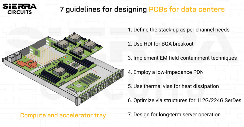
How to Design PCBs for Data Centers and AI Servers
Designing PCBs for AI servers and hyperscale data center platforms requires architectures that support extreme routing density, high-speed serializer/deserializer (SerDes) […]
High Speed
How to Select and Place RF Components for PCB Designs
Choosing the right RF PCB components and placing them appropriately helps you avoid critical issues such as insertion ... more »
PCB Assembly
The Pros and Cons of Composite Amplifiers for PCB Designers
Several manufacturers are making serious efforts in widening the scope of composite amplifiers. The key features of these ... more »
PCB Design
How to Design PCBs for Data Centers and AI Servers
Designing PCBs for AI servers and hyperscale data center platforms requires architectures that support extreme routing density, high-speed ... more »
High Speed
How to Select and Place RF Components for PCB Designs
Choosing the right RF PCB components and placing them appropriately helps you avoid critical issues such as insertion ... more »
PCB Assembly
The Pros and Cons of Composite Amplifiers for PCB Designers
Several manufacturers are making serious efforts in widening the scope of composite amplifiers. The key features of these ... more »
PCB Design
10 Best High-Speed PCB Routing Practices
A PCB designer has a difficult task when it comes to routing a circuit board. Things get a ... more »
High Speed
What Causes High-Leakage Current in PCBs and How to Prevent It?
High-leakage current in PCBs is caused by moisture absorption and inadequate creepage and clearance distances. You can prevent ... more »
PCB Design
Decoupling Capacitor Placement Guidelines Every PCB Designer Should Know
Decoupling is a way of isolating signal components from composite signals based on frequency. Therefore, understanding which range ... more »
PCB Layout
How to Design an ESD Protection Circuit for Your PCBs
An ESD protection circuit safeguards sensitive PCB components from high voltage spikes caused by an electrostatic discharge event. ... more »
PCB Design
How to Select Components and Materials for Power Electronics PCBs
Power electronics PCBs are designed to handle elevated currents and voltages in applications like electric vehicles (EVs) and ... more »
High Current
5 Typical PCB Design Challenges With Solutions for Engineers
With the rapid advancements in AI and IoT technologies, modern circuit designs demand careful attention to electrical, mechanical, ... more »
PCB Design
Fabrication, Procurement, & Assembly. PCBs fully assembled in as fast as 5 days.
- Bundled together in an entirely-online process
- Reviewed and tested by Engineers
- DFA & DFM Checks on every order
- Shipped from Silicon Valley in as fast as 5 days
Fabrication. Procurement & Assembly optional. Flexible and transparent for advanced creators.
- Rigid PCBs, built to IPC-6012 Class 2 Specs
- 2 mil (0.002″) trace / space
- DFM Checks on every order
- 24-hour turn-times available
Complex technology, with a dedicated CAM Engineer. Stack-up assistance included.
- Complex PCB requirements
- Mil-Spec & Class 3 with HDI Features
- Blind & Buried Vias
- Flex & Rigid-Flex boards


