Contents
Sequential lamination is a process of fabricating a circuit board using subsets composed of copper and dielectric layers. This process enables you to incorporate advanced via structures such as stacked and staggered microvias in your HDI PCBs.
In this article, we will explain how sequential lamination is carried out to fabricate microelectronic and high-density boards and the ways to improve their reliability.
What is sequential lamination?
Sequential lamination is the method in which two or more subsets are created individually and bonded together. A subset is part of a multilayer board that goes through the same process as the main board. After preparing them, prepreg sheets are inserted between each pair of subsets, and the complete lay-up is bonded together to build multilayered HDI and UHDI boards.
The number of lamination cycles can range from 2 to more than 4, depending on the complexity of the PCB. This process involves operations such as drilling blind and buried vias and etching signal routes on inner layers. The most significant factors that impact the number of lamination cycles are:
- Starting and terminating ends of blind and buried vias
- Type of construction (foil or core)
Step-by-step process of sequential lamination
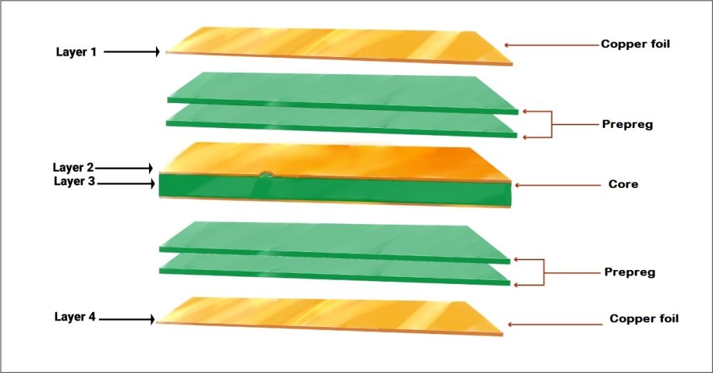
- The stack-up operator places the copper foil (layer 4 in the above image) and prepreg sheets on a heavy steel base plate.
- The pre-treated core (layer 2 and layer 3) is fixed accurately with the help of the alignment pins.
- The operator adds prepreg sheets, copper foil (layer 1), and an aluminum press plate. This plate is used to ensure a smooth copper finish. The first subset is now ready.
- The other subsets are constructed in the same way. Next, these sub-boards are laminated sequentially, imposing prepreg sheets between them to produce a multilayer stack-up.
- The entire lay-up is then rolled under a press to lower the top steel plate.
- The operator ensures the subsets and outer copper layers are accurately registered, using the alignment pins, before sending them to the racks.
- The entire build-up is loaded into a bonding press, where heated press plates with high pressure are used to bond the layers. High-temperature melts and cures the epoxy resin in prepregs.
- The press is cooled down to establish lifetime layer bonding.
- The pressure applied on a board stack-up depends on its cross-sectional area (length x height x width). Typically, for a standard PCB, the pressure is 250 pounds/ sq. inch. The pressure will automatically increase if we load boards with higher cross-sectional areas.
- Once the process is completed, the press operator unloads the stack carefully and removes the aluminum plates.
- To get rid of corrosion, dry film, anti-foam residues, and any fingerprints, panels are scrubbed and cleaned.
For an in-depth knowledge of HDI PCB design considerations, download the HDI PCB Design Guide.

HDI PCB Design Guide
5 Chapters - 52 Pages - 60 Minute ReadWhat's Inside:
- Planning your stack-up and microvia structure
- Choosing the right materials
- Signal integrity and controlled impedance in HDI
- Manufacturing considerations for higher yields
Download Now
Sequential lamination vs. sub-lamination in PCB fabrication
Here’s a quick comparison between sequential lamination and sub-lamination.

Factors to consider in sequential lamination
Choose 2 to 3 lamination cycles for optimum results
Increasing the number of lamination cycles will raise the cost of your board. Always try to keep the number between 2 and 3. This brings down the cost, maintains signal integrity, and increases reliability. However, this approach may not work for advanced HDI boards. In such instances, you need to optimize the number of lamination cycles while realizing the DFM standards. Brings down the cost, maintains signal integrity, and increases reliability.
Read our case study on designing an HDI board with .4 and .65 mm BGAs to understand how we optimized the number of lamination cycles without compromising the design requirements.
Avoid CTE mismatch of the chosen materials
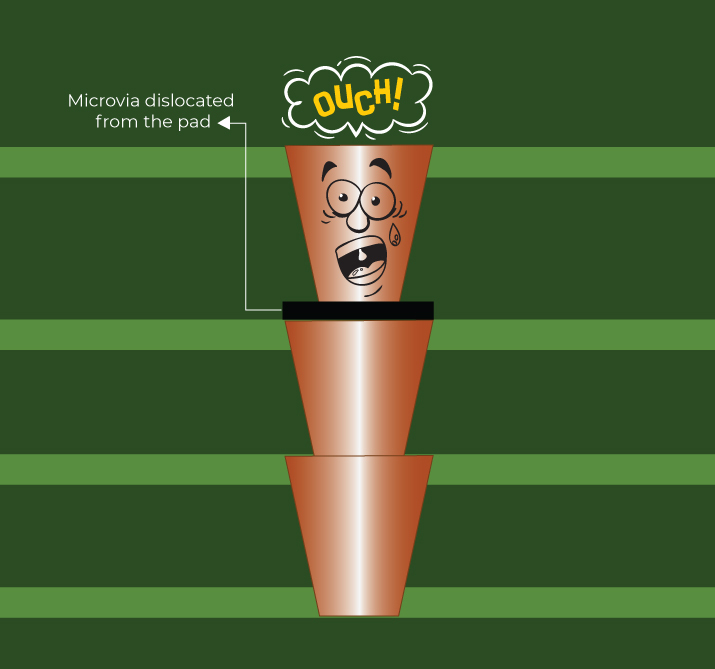
Sequential lamination deals with coefficient of thermal expansion (CTE) problems considerably. It involves greater risks of lamination voids and copper extensions on the Z-axis while encountering high pressure and temperature during bonding.
The CTE of glass reinforcement is around 6 ppm/°C, while the CTE of copper is 17 ppm/°C and the CTE of resin is around 100 ppm/°C. With increasing temperatures, the dielectric material will expand faster than the copper.
In the Z-axis, the resin glass matrix expands 4.5-5 times faster than copper below Tg. The rate of expansion goes up to 17-20 times faster than copper above Tg. This causes the resin to be pulled off of the pad, and the copper pad gets deformed at the edges. The net effect is a huge pressure exerted around the pad. If this pressure exceeds the strength of the resin, delamination occurs. Because each lamination cycle can introduce material shrinkage, manufacturers rely on PCB scaling techniques to maintain accurate layer-to-layer registration in HDI builds.
How to increase the reliability of your HDI
To improve the reliability of your board, you need to reduce the structural stress and distribute heat over a larger area. For this, you need to adhere to the following best practices.
Material selection: Choose a dielectric material with high Tg (≥ 180°C) and low Z-axis expansion to reduce the stress caused by CTE mismatching.
Addition of heat sink: Heat sinks are made of aluminum or copper. Both of these materials have high thermal conductivity and low thermal resistance. Therefore, the sinks can smoothly transfer the heat from the areas with higher thermal resistance to the ones having lower thermal resistance by the conduction method.

Stack-up and fabrication: Incorporate lower resin content for subsets to reduce the Z-axis expansion. On the contrary, for dielectrics, a high resin content is chosen that helps spread the stress over a larger volume. The amount of resin over the copper pad depends on the material hardness.

Materials suitable for high-density interconnects
While selecting the material for your HDI boards, consider the following parameters:
- Glass transition temperature (Tg): ≥ 180°C (typical)
- Dielectric constant (Dk): >5 (If your design has high-speed signals, choose a material with lower Dk to achieve low losses)
- Coefficient of thermal expansion (CTE): < 70°C/ ppm along Z axis
- Loss tangent (tanδ): 0.01 to 0.002 (The lower the loss tangent, the lower the loss)
Always talk to your manufacturer before finalizing the dielectric material. We recommend the following materials for sequential lamination:
Isola-370 HR
This material comprises a multifunctional FR4 epoxy resin with a glass transition temperature of 180°C and a high conductive anodic filament (CAF) resistance. It provides superior thermal performance with low CTE and improved mechanical and chemical resistance and is proven to be the best choice in various PWB applications.
Isola-I-speed
I-speed laminate materials are manufactured with a high-performance, multi-functional resin reinforced with electrical-grade (E-glass) glass fabric. This system delivers a 15% improvement in Z-axis expansion and offers 25% less loss than competitive products in this sector. Additionally, superior moisture resistance during reflow can be attained by using I-speed prepreg.
Panasonic Megtron 6, 7, and 8
Materials in the Megtron family offer high-quality performance and reliability. Megtron 6, Megtron 7, and Megtron 8 are prevalently incorporated to build high-layer-count PCBs for networking and digital communication applications at lower RF frequencies.
Nelco 7000
Nelco-7000 prepreg belongs to a series of toughened polyimide materials and is used to manufacture multilayered boards. This laminate material provides excellent thermal performance and improved reliability. Nelco-7000 supports lead-free assembly compatibility and high-density circuits for defense and aviation applications.
Arlon 85 NT
Arlon 85 NT is a pure polyimide with a high Tg of 250⁰C and reinforced with a non-woven substrate. This prepreg offers high-reliability features in addition to temperature stability, low in-plane expansion of 6-9 ppm/⁰C, and outstanding dimensional stability.
Rogers 4000 and 5000 series
These laminates are made up of hydrocarbon and ceramic. These prepregs dominate the PCB industry because of their superior thermal conductivity, high Tg (around 250⁰C), controlled dielectric constant, and thermal robustness. This low-loss material is preferred over traditional PTFE materials for microwave and millimeter frequency applications.
To know the basics of RF and microwave PCB design, download the RF and Microwave Design Guide.
RF & Microwave Design Guide
8 Chapters - 44 Pages - 60 Minute ReadWhat's Inside:
- Basics of RF and microwave board design
- Choosing RF materials
- Trace, grounding, via, and stack-up design
- Component selection and placement
- Testing and isolation requirements to avoid interference
Download Now
Sample HDI stack-ups
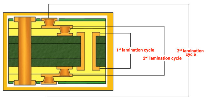
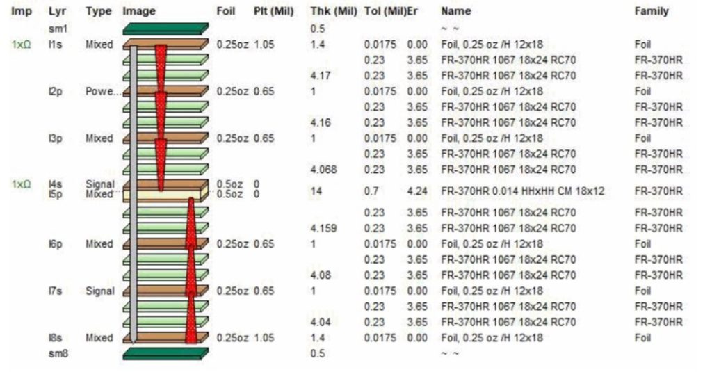
This HDI stack-up contains blind vias from 1-2, 2-3, 3-4, 5-6, 6-7, and 7-8. All these are stacked. Here, you will need to incorporate three lamination cycles after core preparation:
- First cycle: From layers 3 to 6
- Second cycle: From layers 2 to 7
- Third cycle: From layers 1 to 8
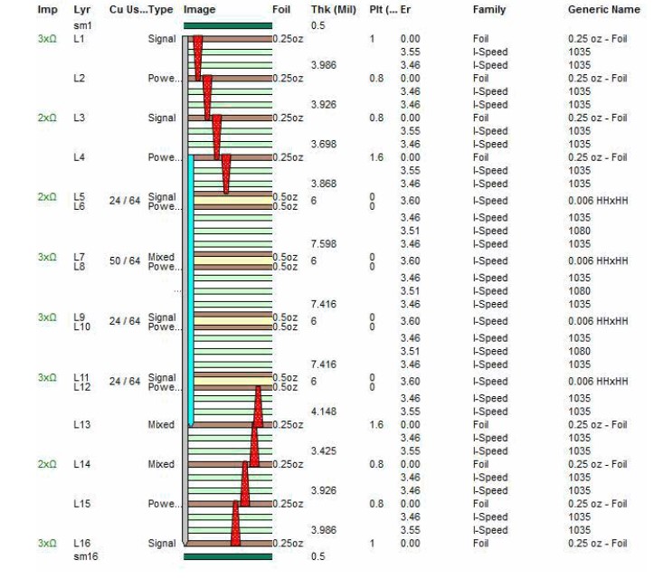
Below stack-up contains blind vias from 1-2 and 15-16. Laser-drilled, buried vias lie between 2-3, 3-4, 4-5, 12-13, 13-14, and 14-15. The HDI structure also comprises a mechanically drilled buried via layers 4 to 13. Hence, the required number of lamination cycles is 4.
- First cycle: From layers 4 to 13
- Second cycle: From layers 3 to 14
- Third cycle: From layers 2 to 15
- Fourth cycle: From layers 1 to 16
Sequential lamination is the most feasible solution to build multiple-layer stack-ups with advanced via structures. It enables complex inner layer routing with blind and buried vias. It also offers an excellent solution to achieve a consistent aspect ratio on all drills.
At Sierra Circuits, we analyze the stack-up, the number of vias on each layer, and the materials before finalizing the number of lamination cycles. If required, the team will optimize the lamination cycle count as per your budget without compromising on the design standards.
Need assistance with building your HDI stack-ups? Post your queries on our forum, SierraConnect. Our HDI PCB experts will answer them.

About Poulomi Ghosh : Poulomi is a microwave engineer specializing in EMI, EMC, RF, and high-speed electronics. As a senior technical writer at Sierra Circuits, she creates advanced engineering articles and webinars for hardware engineers and PCB designers.