


Contents

On-demand webinar
How Good is My Shield? An Introduction to Transfer Impedance and Shielding Effectiveness
by Karen Burnham
A hybrid stack-up construction enhances your PCB’s performance and cost-effectiveness by combining different materials or technologies. It helps you achieve customized electrical, thermal, and mechanical properties for your circuit board design.
Using this technique, you can combine both analog (RF) and digital circuits onto a single board. Typically, a hybrid RF board can have an operational frequency ranging from 2-5 GHz. Beyond this, opt for a pure stack-up with low-loss laminates.
Highlights:
To build a hybrid stack-up:
- Combine materials with different Dk to achieve optimized electrical, thermal, and mechanical performance.
- Use specialized materials only on selected layers to reduce signal loss and overall material costs.
- Maintain consistent layer-to-layer spacing and precise impedance by keeping core height stable during lamination.
- Utilize laminates such as FR-4, PTFE, and hydrocarbon ceramics, often combined with a third ceramic-based material for added performance.
In this article, you will learn how to tackle the challenges of designing a hybrid stack-up.
What is a hybrid PCB stack-up?
A hybrid stack-up is built with specialized material only on selected layers to meet specific design requirements such as signal integrity, heat dissipation, and integration of digital and RF circuitry. The configuration of the materials used depends on your application.
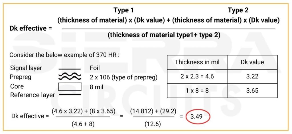
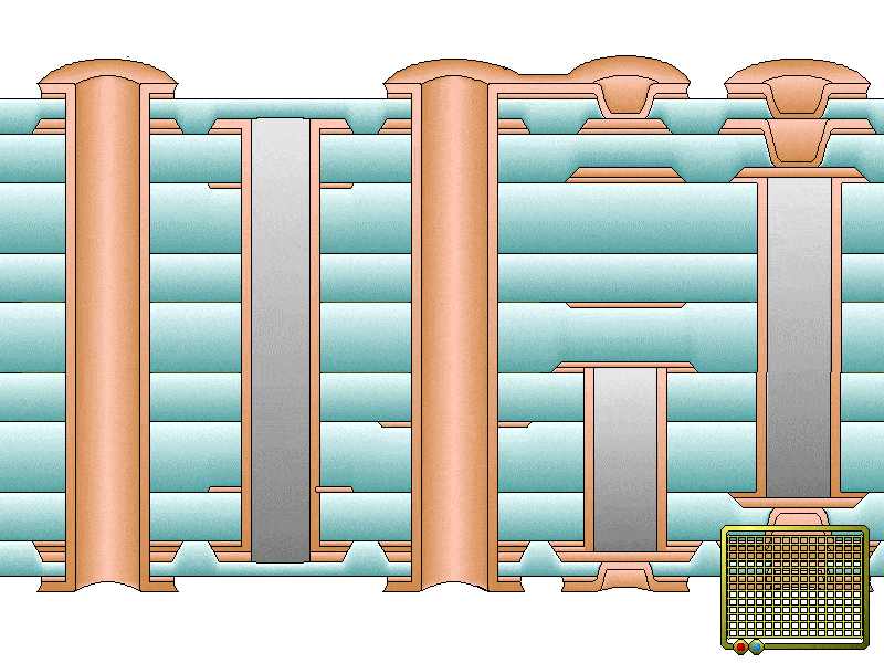
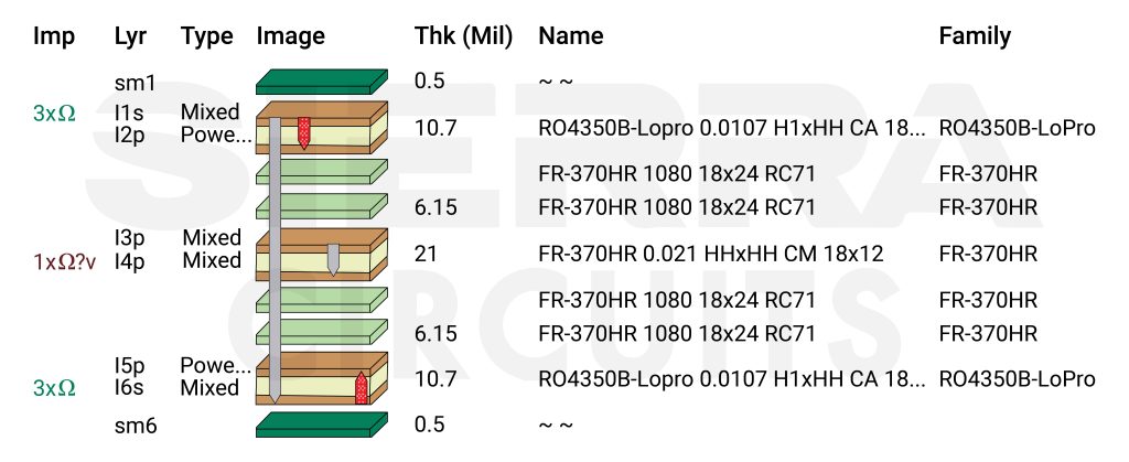
Let’s consider the stack-up below. It is built using Rogers 4350B and Isola FR-370HR. Here, the RF signals are routed on 4350 material as it offers low signal loss at high frequencies.
The cost of materials will be much lower when compared to building an entire board with Rogers 4350B. Due to the use of low-Dk material, the electrical performance will also be enhanced.

Similarly, if you’d like to increase the heat dissipation capability of any selected layers, you can use a metal core or a dielectric material with a higher thermal conductivity.
When do you need a hybrid PCB stack-up?
Opt for a hybrid stack-up construction when integrating different materials or technologies becomes beneficial or helps you overcome design challenges.
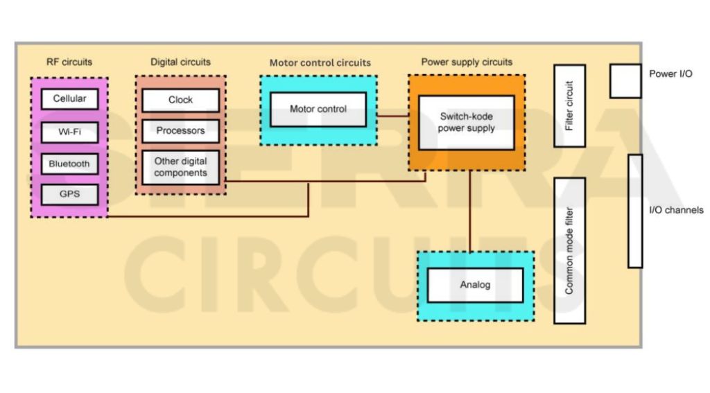
Mixed-signal applications
If sensitive analog and noisy digital signals coexist in the same design, hybrid stack-ups can be used. By this, you can isolate critical signals and improve the signal integrity of your design.
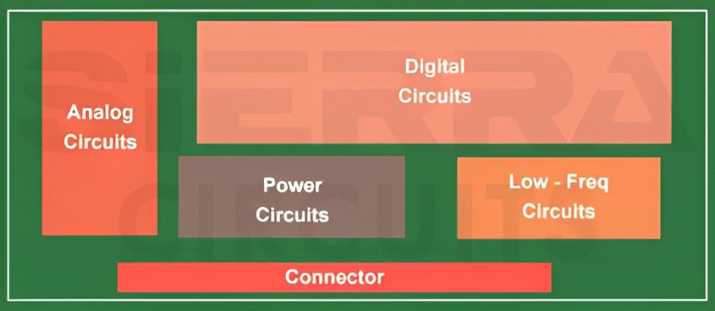
RF/microwave and high-speed designs
In RF and microwave PCBs, precise impedance control is essential. By incorporating a specialized material where RF signals are routed, you can ensure efficient impedance control without increasing the overall cost. In addition to this, a tightly coupled ground plane arrangement will help you create an efficient current return path.
Here’s an infographic on designing hybrid stack-ups for your RF PCBs:
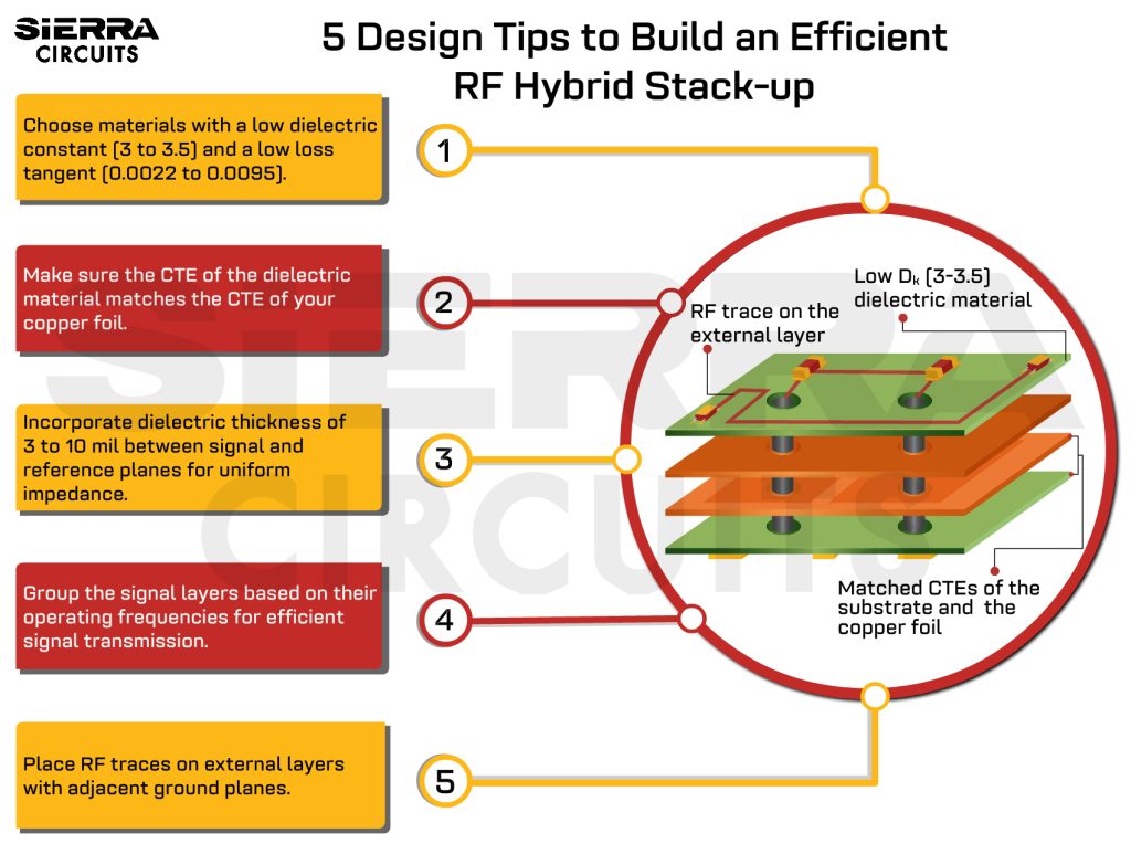
Hybrid PCB stack-ups offer a practical solution for RF designs by combining different laminate materials to balance performance, manufacturability, and cost.

Here are a few reasons why it is commonly chosen for RF applications:
- A hybrid stack-up allows you to have different Dk material in a specific layer of the stack-up. This reduces signal loss and overall material costs.
- The stack-up is easier to laminate, drill, and desmear.
- This configuration helps you maintain consistent layer-to-layer spacing and accurate impedance as the core height remains stable during lamination.
For high-speed designs, you can choose a material with a uniform dielectric constant over a wide range of frequencies on selected layers. By this, you can minimize signal reflections, crosstalk, and EMI.
When using different materials in a hybrid stack-up, be cautious of mismatched CTE values, not just through the Z-axis but also across the XY plane due to copper distribution. These mismatches can cause mechanical stress during thermal cycles.
To avoid redesigns, always validate your material choices with your PCB fabricator early in the design process.
For more stack-up design tips, download our e-book.
PCB Stack-Up Design Guide
12 Chapters - 55 Pages - 60 Minute ReadWhat's Inside:
- Design guidelines for HDI, flex, and hybrid stack-ups
- Stack-up representation in fab drawing
- DFM checks for layer stacks
- Characteristics of high-speed materials
- Manufacturing tolerances
- PCB stack-up examples with illustrations
Download Now
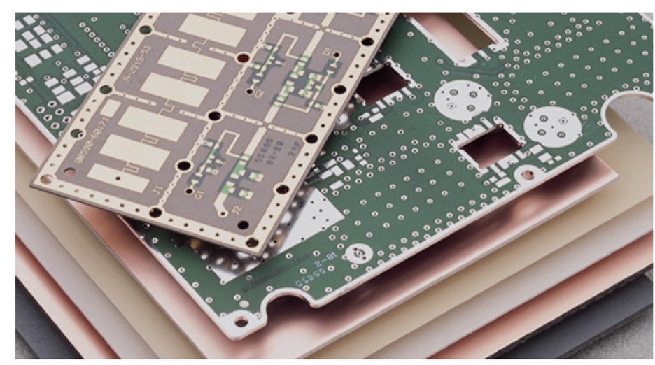
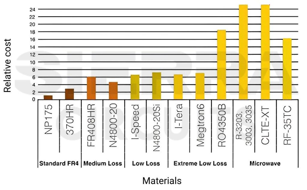
PCB materials utilized in hybrid stack-ups
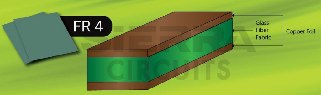
Usually, the main laminates used for fabricating hybrid boards are FR-4, PTFE, and hydrocarbon ceramics. They are compatible and sometimes integrated with a third ceramic-based material. However, you may have to modify the dielectric formula to achieve the desired Df and Dk values for specific applications.
FR-4 material
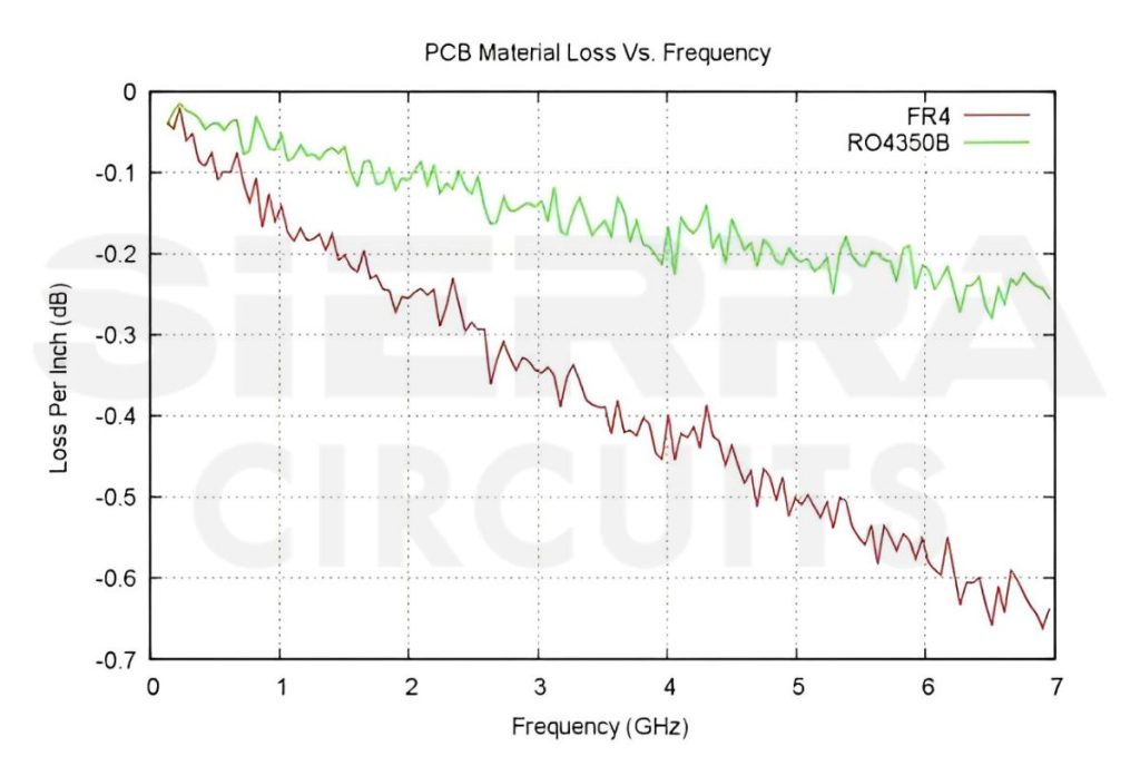
It is a widely used laminate due to its affordability and excellent properties. However, it is not preferred for high-frequency operations due to higher signal loss. Hence, it is often combined with low-Dk materials to build high-speed and RF boards. The specialized laminate should have the following qualities:
- Uniform impedance control
- Better heat conductivity
- Uniform dielectric constant and dissipation factor over a wide range of frequencies
Other specialized materials
Polytetrafluoroethylene (Teflon): PTFE offers improved impedance control and low signal loss. It is best suited for high-frequency boards. However, PTFE can be expensive when compared to FR-4.
They can also experience dimensional changes, as it is a softer material. A special via treatment process is required for these substrates. Manufacturers like Rogers, Nelco, Arlon, and DuPont produce PTFE-based laminate.
Ceramic-filled PTFE: RT/duroid (5870, 5880, 5880LZ, and 6002) and RO3000 ( RO3003, RP3003G2, RO3006, RO3010) are a few examples of ceramic-filled PTFE material. They exhibit reduced signal losses and have a stable dielectric constant. They also have higher structural stability.
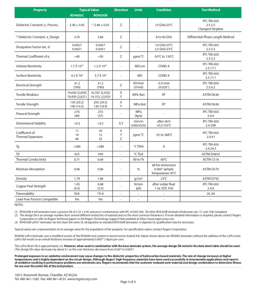
Hydrocarbon ceramics: RO4000 laminates (RO4000 LoPro®, RO4003C, RO4350B) are hydrocarbon ceramic-based laminates. They have a low dielectric constant, and their manufacturing process is similar to FR-4. The CTE is similar to copper; hence, they have good dimensional stability during fabrication.
Bonding material
Standard adhesives cannot be used when bonding dissimilar materials. You need to choose a bonding material with low lamination and re-melting temperatures. The overall thickness of the stack-up should be calculated along with the bonding material.
Typical bond plies include fluorinated ethylene propylene (FEP), ceramic-filled PTFE, and liquid crystal polymer (LCP). Always get insight from your manufacturer on the type and thickness of adhesive material.
Hybrid stack-ups are cost-effective only when one type of prepreg is used to bond hybrid cores. For example, Roger 4350 and 370HR cores are bonded with 370HR prepreg. If you use multiple prepregs of different materials, it can drive up the cost and manufacturing time.

How to design an efficient hybrid stack-up
- Define the design requirements, such as high-frequency operations, controlled impedance, power delivery, thermal management, and mechanical constraints.
- Determine the appropriate layers and materials based on the design expectations. Consider the dielectric constant, dissipation factor, thermal conductivity, and CTE.
- Compute the total number of signal layers based on component density, via requirements, board, and trace dimensions.
- Group the signal layers based on their operating frequencies and sensitivity to interference. Assign layers with special materials to isolate them from the rest.
- Place the RF signals on the top layers with adjacent ground planes.
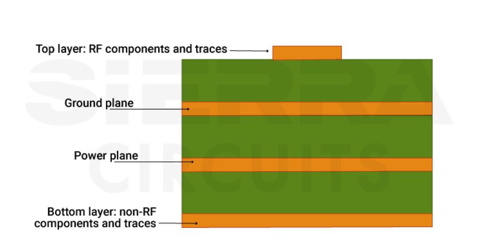
RF trace routing in hybrid stack-up To learn how proper layer orientation improves signal integrity and reduces EMI, read PCB layer orientation.
- Place the power plane right below the ground plane to achieve a low-inductance path for current flow.
- Strategically plan the dielectric spacing between the signal, power, and ground layers to manage impedance control, crosstalk, and electromagnetic compatibility (EMC).
- Verify the performance of your stack-up design using simulation tools.
Hybrid buildup representation in Gerber
Conveying the stack-up information in the standard format is especially crucial in a hybrid stack-up. The various materials used and their thickness should be clearly mentioned to guide your fabricator in the right direction.
- Create a detailed stack-up cross-section specifying the layer order, materials, thicknesses, copper weights, and overall board thickness.
- Mention the different materials used, layer names, types, and thicknesses in the fabrication drawing.
- Write about dielectric material specification, controlled impedance requirements, manufacturing tolerances, testing, and report details in the fab notes.
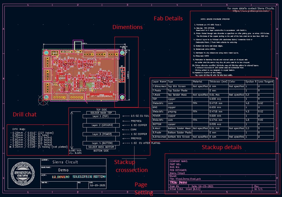
- For controlled impedance, mention the impedance value, targeted layer, and allowed tolerance. The manufacturing tolerance for stack-up includes layer-to-layer registration, board thickness, bow, and twist.
- To ensure the stack-up is manufactured as per your design, you can request a cross-section analysis. It will include details such as the dielectric thickness of each layer, copper plating on the outer layers, copper thickness on the inner layers, hole diameter, and plating.
5 benefits of a hybrid stack-up
Hybrid PCB stack-ups offer numerous advantages, such as improved signal propagation and the performance of the circuit board. Some of them are listed below:
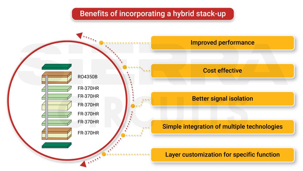
1. Layer customization to meet specific design requirements
Every hybrid stack-up is customized and optimized to realize your design requirements. For example, each layer can be tailored for specific functions such as signal integrity, power distribution, and thermal management. This improves performance and reliability without increasing the overall cost.
2. Cost-effective in high-volume production
By strategically utilizing different materials and layer configurations, we minimize the use of expensive materials or complex manufacturing processes. Building a board completely with low Dk material may not create a huge cost difference in prototyping. When it comes to high-volume production, cost becomes a crucial factor.
3. Signal isolation and noise reduction
A hybrid stack-up enables you to isolate sensitive analog or digital signals from noisy components. More importance is given to ground planes, power planes, and shielding layer arrangements to reduce the impact of noise and crosstalk.
4. Better thermal management
The specialized material selected for your stack-up can have better heat dissipation capacity. You can also incorporate special thermal planes or additional copper layers to improve the board’s thermal properties. This is crucial for high-power applications as it improves the lifespan of the PCB and its components.
5. Easy integration of multiple technologies
Different functionalities, such as analog and digital circuitry, RF components, sensors, and microcontrollers, can be consolidated effectively. Hence, the system integration becomes simpler, reducing complexity and the size of the board.
Need help in designing reliable PCBs? Our engineering team can help you with thermal management, stack-up design, and DFM analysis.
You can book a meeting with our experts or call us at +1 (800) 763-7503.

Challenges in building a hybrid stack-up
Combining different materials and technologies increases the risk of layer registration, separation, and delamination issues. When designing a hybrid stack-up, you need to consider the following factors:
Layer registration issue due to different CTE
Different CTE properties of different materials used in hybrid PCBs can cause registration issues during fabrication and component assembly. The manufacturer applies thermal pressure during the lamination process, which can cause expansion or contraction mismatches.
Consider a hybrid PCB layer stack with PTFE material and FR-4. This buildup has the risk of deforming permanently during thermal cycling. PTFE has a higher CTE value compared to FR-4. Hence, the FR-4 section of the stack-up rises above the Tg value and expands rapidly, which can deform the board permanently.
To avoid this issue, you need to know the technical details of the materials used. You can find material data sheets and technical information from global laminate manufacturers like Isola, Rogers, Panasonic, and others. These will also be available at your fab house. When combining materials with different CTE values in hybrid stackups, accurate PCB scaling becomes essential to counteract differential shrinkage during lamination.
IPC standard for laminate selection provides guidelines on Tg, Td, Dk, and CTE for different base materials in the 4101 standards. Following this information can help you choose the right dielectric for the stack-up. You can also perform a material compatibility test.
To learn how to select the right materials for your high-speed PCBs, download our design guide.
High-Speed Material Design Guide
6 Chapters - 19 Pages - 30 Minute ReadWhat's Inside:
- Importance of choosing the right material for your high-speed design
- Parameters that affect material selection
- Effect of dielectric constituents on your circuit board
- Characteristics of high-speed materials
- Effect of resin content and glass weave structure on your PCB
Download Now
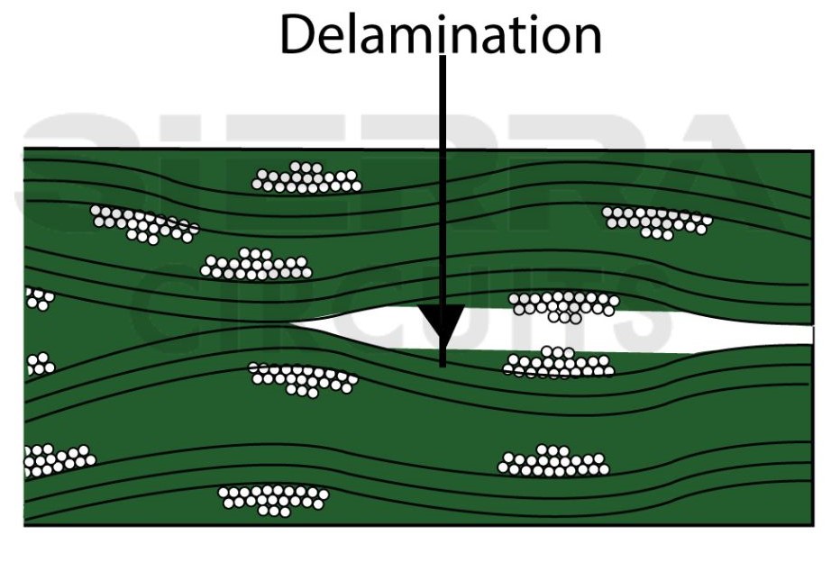
Layer separation and delamination
Hybrid stack-up construction can increase the risk of layer separation and delamination. This can hamper the circuit board’s structural integrity and performance. To mitigate this issue, ask your CM to plan the lamination process according to the delamination periods of the materials used. Bonding materials and techniques must also be compatible with the chosen materials.
Lamination issues due to varied layer thicknesses
Selecting an optimum layer thickness for each material by considering the operating frequency is critical. In hybrid stack-ups, materials will have different insulation and adhesion properties. This can lead to lamination issues. To avoid this, always seek your fabricator’s opinion before you finalize the thickness of the chosen materials.
Uneven plating due to the different hole preparation processes
The drilling speed and mechanical strength required for via creation vary with materials. The processes and chemicals used for hole preparation may also differ.
For instance, if you use PTFE material in a hybrid stack-up, it needs to undergo plasma etching to de-smear drilled holes before plating. This process will have a higher etch rate on FR-4, which results in an uneven surface for plating. To overcome this challenge, via plating should be thicker.
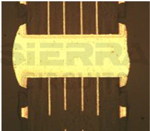
Further, the dissimilar materials can shrink or expand during the sequential lamination, which can offset drilled holes. Here’s an example of an HDI hybrid buildup.
Key takeaways
- To avoid layer registration, choose materials with equivalent CTE
- Consult your CM before finalizing the layer thicknesses in your hybrid stack-up
- Increase the via plating thickness to reduce the risk of uneven plating
Here’s what Laurent Nicolet, the Vice President of Business Units Electronics at the Schmid Group, has to say about the future of PCB etching.
Importance of collaborating with experienced manufacturers
Fabricating a hybrid board requires expertise and experience, as it consists of different materials. Finding a manufacturer capable of building your board is essential.
When you include dissimilar materials in your stack-up, it is best to contact your fabricator at an early stage to ensure design success. Before designing, take their recommendations on material selection and the fabrication process. Later, check if it is possible to build the designed stack-up without any DFM issues.
Sierra Circuits has experienced and skilled design engineers who can help you select the right materials for your hybrid buildup. See our RF PCB and microwave prototype services to learn more.
Need assistance in designing your hybrid stack-up? Post your queries on SierraConnect, and our design experts will resolve them.

About Sushmitha V : Sushmitha V has a master's degree in power electronics and has over four years of experience in the PCB industry. Her areas of interest include circuit board manufacturing, assembly, IPC standards, and DFM/DFA practices.


Start the discussion at sierraconnect.protoexpress.com