


Contents

On-demand webinar
How Good is My Shield? An Introduction to Transfer Impedance and Shielding Effectiveness
by Karen Burnham
We previously quickly discussed signal reflection in our PCB transmission line article. This is an in-depth article about this very important topic that PCB designers should master. The first thing to remember is that signal reflection in PCB transmission lines occurs due to impedance discontinuity.
A transmission line should have a uniform characteristic impedance. Any variation or discontinuities to the impedance causes signal reflection and distortion.
This phenomenon is equally true for PCB traces and transmission lines. The reason for this is that the physical wavelength of a high-frequency signal is very short. For that reason, PCB traces exhibit the same characteristics. The higher the frequency, the shorter the wavelength. You must even treat shorter traces like transmission lines.
Signal trace discontinuities or non-uniform discontinuities form signal integrity discontinuities. In order to avoid signal distortion at the source and destination, you must match the PCB trace impedance to source. You must then load impedance at the source and destination ends. This presents a considerable challenge that requires careful PCB design to mitigate the effects of signal degradation caused by impedance discontinuity. The greater the discontinuity in the characteristic impedance, the higher the signal reflection. This means the signal distortion is higher as well. As such, try and keep impedance discontinuities as minimal as possible. Both in terms of amplitude and time. Read: why controlled impedance really matters.
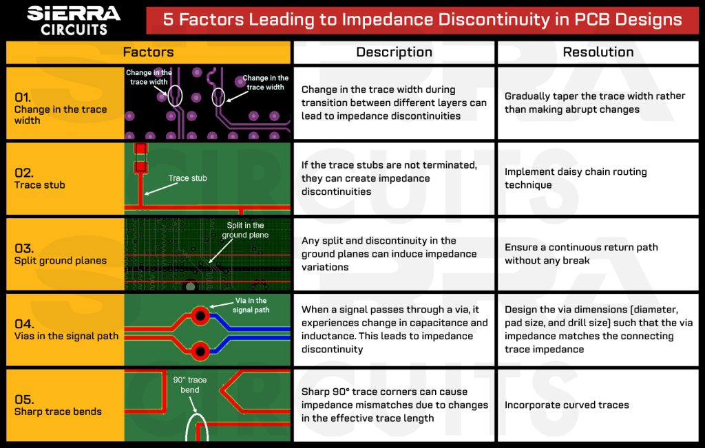
Discover the key factors behind impedance discontinuity in PCB designs with our infographic: 5 factors leading to impedance discontinuity in PCB designs.

Impedance Discontinuities Affect Signal Integrity
A digital signal is, in theory, a square wave pulse that switches in a very short time. It naturally follows that the short signal rise times required by high-frequency digital circuits will result in extremely high frequencies associated with fast signal rise times. In practice, these frequencies will be an order of magnitude higher than the circuit’s clock frequency. High-frequency digital circuits would have a shorter pulse width. And thereby even shorter rise times. A very short signal rise time implies very high frequencies contained in the digital signal. Therefore, high-frequency digital signals should follow the signal integrity discipline associated with high-frequency signals.
Consequently, any change in the impedance of a PCB trace will cause signal reflections. These lead to circuit board ringing and signal distortion. The upshot of this is that, at high switching frequencies, the distortion this causes to digital signals by impedance discontinuities can be so severe that signal sampling errors may occur. You can characterize a transmission line formed by PCB traces by the following parameters: resistance, conductance, and trace resistance. Read the difference between microstrip and stripline in PCBs.

High-Speed PCB Design Guide
8 Chapters - 115 Pages - 150 Minute ReadWhat's Inside:
- Explanations of signal integrity issues
- Understanding transmission lines and controlled impedance
- Selection process of high-speed PCB materials
- High-speed layout guidelines
Download Now
Typical Impedance Discontinuities
The characteristic impedance of a line is the square root of the inductance divided by the capacitance. This is a reasonable assumption for PCBs because trace resistance and conductance at high signal frequencies are negligible compared to their inductance and capacitance.
An impedance discontinuity is anything that affects the ratio between the inductance of the trace and its capacitance. Here are some typical examples:
-
- Impedance variation in the line: If the impedance of a line changes for any reason, such as due to a change in copper section or a variation in the trace path, the mutual inductance changes, and impedance discontinuity will occur.
- Branches in traces: Although it may be necessary to route a signal to more than one device, the use of branches and line stubs change the line impedance, causing a discontinuity.
- Splits in return signals: A high-frequency signal follows the path of lowest impedance, which is directly under the signal trace, often in a ground plane. Any physical feature in the return line or ground plane that forces the return signal to deviate from this route will create a discontinuity.
- Vias: Use a via to transfer a signal from one layer in a PCB to another. Although an essential feature of PCB design, the shape and size of a via changes the inductance and capacitance of the trace, creating another discontinuity. To learn more, read how to reduce parasitic capacitance in PCB layout.

How To Limit the Effects of Impedance Discontinuity
The key to controlling the negative effects of impedance discontinuities is to treat all PCB signal traces as transmission lines. You should ensure that the characteristic impedance is the same at all points of the signal path.
Make sure you follow these guidelines:
-
-
- Match source and load impedances: Ensure the source and load impedances are the same as the trace impedance. You can achieve this through the use of series or shunt resistors to realize the correct impedance. Additionally, you must terminate any open traces using a resistor of the correct value.
- Avoid branches: If signals have to be shared by several chips, daisy-chain the traces to connect the circuits in preference to using branches. Alternatively, a matched buffer device could be used to transfer the signal to a branch.
- Signal return paths: Make sure that signal returns follow the same route as the signal line. If using a ground plane, ensure there are no splits that interrupt the return signal path. Ensure there is a solid plane underneath the trace through the entire length with no splits or cuts. If there is no solid plane, use a thick return trace, which should cover the trace lengthwise and the height of the dielectric three times over.
- Via design: Layout the high-frequency traces on one layer as far apart as possible. If vias are required, use microvias instead of traditional vias. Because vias have significantly different capacitance and inductance characteristics, minimize their use on signal traces. Where they are required, use microvias that have a much smaller capacitance and inductance of standard vias. The microvia also help keep the stub length as short as possible. An alternative is to use high-density interconnect or HDI PCB technology.
-
The detrimental effects of impedance discontinuities are severe. You can’t ignore them in digital PCB circuits operating at high clock frequencies. You should be careful when controlling these effects by adhering to sound design practices and, where possible, using advanced PCB design software to assess and reduce impedance discontinuities.
Impedance Discontinuity and Signal Reflection
A signal on a uniform transmission line encounters a constant impedance ‘Zc (V/I)’ at all locations on the line and the signal travels as desired along it. However, if there is an impedance discontinuity at any point, the signal travel will be affected and signal reflections will occur just like light is reflected when it encounters a discontinuity in medium through which it travels.
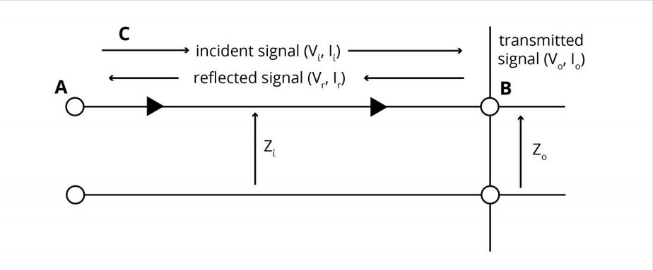
Let’s say that from point A to point B, the line is uniform with impedance ‘Zi’; but at B, there is an impedance discontinuity and the line impedance changes at B and beyond to ‘Z0’.
Let’s say that a signal is sent from A on the line (of impedance ‘Zi’) towards B. At B, let the incident signal voltage and current be ‘Vi’ and ‘Ii’. Then, we must have:
Vi = Zi I0 (1)
Now, if we look at B from the right-hand side where the line impedance is ‘Zo’, then the transmitted voltage ‘Vo’ and the transmitted current ‘I0’ at this point B must be related by:
V0 = Z0 I0 (2)
It needs to be emphasized that relations (1) and (2) are fundamental to the concept of impedance and must always be obeyed.
Given the values of ‘Vi’, ‘Zi’ and ‘Zo’, the problem is to find the value of ‘Vo’.
Case 1: Z0 = Zi, (i.e. no discontinuity in the impedance of the line)
In this case, both the above equations (1) and (2) will be simultaneously satisfied by:
V0 = Vi and I0 = Ii
This is to be expected, as in this case, point B is basically any point on a uniform transmission line, so that at every point B on this line, the transmitted signal will equal the incident signal.

Case 2: Z0 ≠ Zi, (i.e. there is an impedance discontinuity in the line)
Here, if look at both the equations (1) and (2), since Z0 ≠ Zi, it is easy to conclude that we cannot have both Vi = V0 and Ii = I0; because, if for a moment we assume that Vo = Vi, then Ii ≠ I0; and if we assume that Ii = I0, then Vo ≠ Vi. Thus we reach the conclusion that at an impedance discontinuity, the incident signal is not fully and completely transmitted onwards.
The only way we can solve this problem satisfactorily is by assuming that a part of the incident signal is reflected back at the point B of impedance discontinuity, and this reflected signal is superimposed on the incident signal at point B and one the line to the left of it; and at point B, the result of the incident signal and the superimposed reflected signal will equal the transmitted signal at point B.
Let’s therefore say that a part of (Vi,Ii) is reflected back onto the ‘Zi’ transmission line at point B. Let’s represent the reflected signal’s voltage and current at point B by (Vr,Ir).
Therefore at point B, the resulting signal voltage due to incident voltage Vi and the reflected voltage Vr would be (Vi + Vr), and as per Kirchhoff Law applied at point B, this must equal ‘Vo’:
V0 = Vi + Vr (3)
And the resulting current due to the superposition of the incident current ‘Ii’ and the reflected current ‘Ir’ (which is in a direction opposite to that of the incident current) would be (Ii – Ir), and as per Kirchhoff Law applied at point B, this must equal ‘Io’:
I0 = Ii – Ir (4)
And the reflected (Vr,Ir) signal is traveling on the line with impedance ‘Zi’, we must have:
Vr = Zi Ir (5)
Using equations (1), (2), and (5) in equation (3), we have:
Z0I0 = ZiIi + ZiIr = (Ii + Ir)
And since, as per (4), I0 = (Ii – Ir), we have:
Z0 (Ii – Ir) = Zi (Ii + Ir)
Or Ii (Z0 – Zi) = Ir (Z0 + Zi)
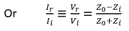
Vr/Vi or Ir/Ii indicates the fraction of the incident signal that is reflected back at point B of impedance discontinuity and is called the reflection coefficient ‘Rc’:
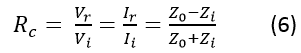
In terms of ‘Rc’, the transmitted signal voltage and current at point B are given by:
Vo = Vi + Vr = (1 + Rc) x Vi (7)
And: Io = Ii – Ir = ( 1 – Rc) x Ii (8)
From the above it is clear that the value of reflection coefficient ‘Rc’ depends on the relative values of ‘Zi’ and ‘Zo’; greater the difference between them, more is the amount of reflection. It can be safely concluded that, in case of impedances being purely resistive, the range of values of ‘Rc’ can be given by:
-1 ≤ Rc ≤ 1
And if Z0 > Zi, a partial positive signal is reflected back leading to a voltage overshoot at B in a pulse signal. And if Z0 < Zi, a partial negative signal is reflected back leading to a voltage undershoot at B in a pulse signal.
We can now discuss some special cases of relative magnitudes of the ‘Zi’ and ‘Zo’.

PCB Transmission Line eBook
5 Chapters - 20 Pages - 25 Minute ReadWhat's Inside:
- What is a PCB transmission line
- Signal speed and propagation delay
- Critical length, controlled impedance and rise/fall time
- Analyzing a PCB transmission line
Download Now
Case (i): Transmission line terminated by its impedance
Here Z0 = Zi (as the transmission line is terminated at its far end B by an impedance of value ‘Zi’), and this leads to: Rc = 0 i.e. there will be no reflection, and the incident signal will be fully transmitted to the far end B. This case tells us how to avoid reflections in a transmission line: simply by terminating the transmission line at the destination by an impedance equal to the impedance of the transmission line.
Case (ii): Transmission line open at the far end
Here Z0 = ∞ (since the transmission line is open at its far end B), leading to Rc = 1. This means that the incident signal will be fully reflected so that V0 = 2Vi and I0 = 0. This means that the superimposed signal voltage will be twice the incident voltage, and the superimposed signal current will be zero, as should be expected at the open end.
Case (iii): Shorted transmission line
Here Z0 = 0 (since the line is shorted at the far end B), leading to Rc = -1 so that V0 = 0 and I0 = 2Ii. This means that a negative of the full incident signal is reflected back to make voltage zero at the shorted end as expected.
Case (iv): When Zo≠ Zi but the difference is small
If ‘Zo’ differs from ‘Zi’ by ~ 20%, the reflection coefficient ‘Rc’ will be ~ 10%, implying that about 5% of the incident signal will be reflected. In most circuit designs, a 10% distortion in signal due to impedance mismatch is acceptable due to the available noise margins.

Various types of impedance discontinuity and their possible causes:
Since the impedance of a transmission line depends on the geometry of the conductors and the PCB material properties, any change in those will cause a change in impedance. Some instances are listed here:
- At the source or the destination/end of the line. Source or receiver impedance is most often not the same as that of the line.
- Change in line width or height (i.e. copper thickness) or change in height and/or dielectric constant of the PCB material between the signal line and return path.
- Vias in the signal trace paths: Vias most often do not have the same impedance as the signal traces – not many designers try to find out what the via impedance is. The saving grace is that the via length is small, so its effect will be in the form of a blip. The start of the via will introduce one reflection, then the end of the via will introduce another reflection. If the via impedance is smaller than the line impedance, this will cause a small undershoot blip in the signal voltage. For very high-speed signals, vias impedance discontinuity does matter greatly, and designers will be well advised to avoid them in critical signal lines, and if necessary, avoid them in the middle of the lines – rather have them near the source and/or destination so that they can be taken care of along with source and destination impedance discontinuities.
- If a signal line is branching into several destinations, at the points of branching, we would see the impedance discontinuities. If a signal line is tapped at various points along its path, there will be impedance discontinuities at the points of tappings.
Multiple reflections:
Consider a transmission line whose length is such that the total propagation time over it is ‘tp’ and let its impedance be 50 ohms. At the source end, it is connected to a source of impedance 16.67 ohms and at the destination, it is connected to a load of 150 ohms. The reflection percentage at the source will, therefore, be -50% and at load it will be +50%.
A 1V signal launched by the source will be reduced to 1V x 50/(16.67+50)= 0.75V on the line at time 0. At time ‘tp’, this 0.75V signal will reach the destination whence 50% i.e. 0. 375V will be reflected back, making the load voltage = 1.5×0.75 = 1.125V. Now, 0.375V reflected signal will reach the source at time ‘2tp’, where -50% i.e. -0.1875V signal will be reflected towards the load. This will reach the load at time ‘3tp’, where 50% of this = -0.0938V will be reflected, thus adding -0.1875-0.0938 = -0.2813V to the old load voltage of 1.125V, making it now = 0.8438V.
Meanwhile, the reflected signal of -0.0938V will reach the source at time ‘4tp’, where -50% of it = +0.04688V will be reflected towards the load; that will reach the load at ‘5tp’, where +50% of it = +0.02345V will be reflected back, thus adding +0.04688V +0.02344V = + 0.07032V to the load, making load voltage now = 0.9141V. Meanwhile, a reflected signal of strength +0.02344V will reach source at time ‘6tp’, of which -50% i.e. -0.01172V will be reflected to reach the load at ‘7tp’, where its +50% will be reflected back, adding a -0.01172Vx150% = -0.01758V to the load making the load voltage now = 0.9141V-0.01758V= 0.8965V. and so on… So the signal at the destination will look like:
From 0 to tp: 0V
tp to 3tp: 1.125V
3tp to 5tp: 0.8438V
5tp to 7tp: 0.9141V
7tp to 9tp: 0.8965V
Thus we will see ringing in the signal at the destination. Ringing with overshoot and undershoot will occur if the source impedance is less than the line impedance causing a negative reflection at the source, and destination impedance is higher causing a positive reflection at the destination.
For more design information, check with our DESIGN SERVICE team and visit our controlled impedance PCB capabilities page.

Controlled Impedance Design Guide
6 Chapters - 56 Pages - 60 Minute ReadWhat's Inside:
- Understanding why controlled impedance is necessary
- Stack-up design guidelines
- How to design for impedance
- Common mistakes to avoid
Download Now
About the author: Atar Mittal is the Director and General Manager of design and assembly division at Sierra Circuits. He is responsible for the design and development of strategies and process automation tools for complex printed circuit boards and assemblies. Atar is also currently engaged in the development of productivity tools for electronics designers that would have a tremendous impact on shortening the development time.
About Atar Mittal : Atar Mittal is the General Manager and Director of the Design and Assembly Sierra Circuits division. He has a degree in Electrical Engineering from IIT Kharagpur and has worked in the electronics industry for over three decades.


