


Contents

On-demand webinar
How Good is My Shield? An Introduction to Transfer Impedance and Shielding Effectiveness
by Karen Burnham
Selecting the right PCBs for IC integration depends on the chip’s signal characteristics, power demands, and the end product. The printed board must meet the IC’s electrical, thermal, and mechanical requirements while ensuring manufacturability and long-term reliability.
As a circuit board designer, knowing how different chip types, packages, and integration levels work with various board technologies helps you choose the right printed board. This leads to better electrical performance, easier manufacturing, and more reliable hardware in the long run.
Highlights:
For successful IC integration:
- Match the board type to the microcontroller unit (MCU) complexity. For instance, use HDI or multilayer boards for microcontrollers with high bit or pin counts.
- Choose multilayer, HDI, or metalcore boards to handle power density and heat dissipation effectively.
- Utilize rigid-flex PCBs to support high-pin-count FPGAs by placing the IC on the rigid section and routing high-speed signals through the flex regions to minimize connector impedance.
- Use low-loss, high-frequency substrates to maintain signal integrity across wide bandwidths.
In this blog, we’ll cover major chip manufacturers to help you make informed sourcing decisions, followed by an overview of chip architectures. You’ll also learn which board types are best suited for different IC categories based on application and complexity, and their DFM and DFA rules.
1. Leading chip designers and manufacturers
1.1. US-based chip design and fabrication companies
The table below provides key information on leading U.S.-based chip designers and manufacturers, including their locations and specialties.
| Role | Company | Headquarters | Focus areas |
|---|---|---|---|
| Designer and manufacturer | Intel | California (Santa Clara) | CPUs, GPUs, chipsets (global fabs in USA, Ireland, and Israel) |
| Texas Instruments | Texas (Dallas) | Analog, embedded processors | |
| Micron Technology | Idaho (Boise) | DRAM, NAND memory | |
| Analog Devices | Massachusetts (Wilmington) | Analog/mixed-signal ICs | |
| ON Semiconductor | Arizona (Phoenix) | Power, automotive, IoT chips | |
| Microchip Technology |
Arizona (Chandler) |
Microcontrollers, analog, mixed-signal | |
| Wolfspeed (formerly Cree) |
North Carolina (Durham) |
SiC, GaN power, and RF semiconductors | |
| Foundry (manufacturer only) | GlobalFoundries |
New York (Malta) |
Foundry services for fabless companies (AMD, Qorvo, Skyworks Solutions, etc.) |
| Designer (fabless) | NVIDIA | California (Santa Clara) | GPUs, AI, data center chips |
| AMD | California (Santa Clara) | CPUs, GPUs, FPGAs (via Xilinx acquisition) | |
| Qualcomm | California (San Diego) | Mobile SoCs, modems | |
| Apple | California (Cupertino) | Custom A/M chips | |
| Broadcom | California (Palo Alto) | Networking and wireless chips | |
| Marvell Technology | California (Santa Clara) | Storage, networking, 5G chips | |
| Synaptics | California (San Jose) | Touch, display, biometric chips | |
| Qorvo | North Carolina (Greensboro) | RF solutions for wireless, defense | |
| Skyworks Solutions | Irvine (California) | RF chips for wireless devices |
Also read, Why Do PCBs Cost Less in China Than in the USA?
1.2. Global IC designers and foundries
The table below outlines major global chip designers and manufacturers, highlighting their headquarters and core areas of expertise.
| Role | Company | Headquarters | Focus areas |
|---|---|---|---|
| Designer and manufacturer | Samsung Electronics | South Korea (Suwon) | DRAM, NAND, SoCs, and foundry services |
| NXP Semiconductors | Netherlands (Eindhoven) | Automotive, industrial, IoT chips; secure connectivity solutions | |
| STMicroelectronics | Switzerland (Geneva) | Analog, microcontrollers, MEMS | |
| Infineon Technologies | Germany (Neubiberg) | Power electronics, automotive chips | |
| Foundry (manufacturer only) | TSMC | Taiwan (Hsinchu) | Largest independent foundry (Apple, AMD, etc.) |
| UMC | Taiwan (Hsinchu) | Mature-node foundry services | |
| SMIC | China (Shanghai) | Semiconductor foundry (China’s largest) | |
| Tower Semiconductor | Israel (Migdal Haemek) | Analog and specialty foundry | |
| Designer (fabless) | MediaTek | Taiwan (Hsinchu) | Mobile SoCs, WiFi chips |
| HiSilicon (Huawei) | China (Shenzhen) | Develops Kirin processors (limited by sanctions) | |
| ARM | UK (Cambridge) | Licenses CPU/GPU IP to other designers |
Download our design guide for DFA tips.

Design for Assembly Handbook
6 Chapters - 50 Pages - 70 Minute ReadWhat's Inside:
- Recommended layout for components
- Common PCB assembly defects
- Factors that impact the cost of the PCB assembly, including:
- Component packages
- Board assembly volumes
Download Now
2. 5 key chip architectures and their applications
In the semiconductor world, architecture refers to the instruction set architecture (ISA), a framework that defines how a chip processes data, executes instructions, and manages memory and registers.
Here are 5 key semiconductor architectures, their applications, and AI hardware PCBs for chip integration.
- x86 / x86-64: A complex instruction set computing (CISC) architecture developed by Intel and AMD, known for high performance and broad software compatibility. This architecture calls for robust power delivery networks and advanced cooling strategies as it generally comes in dense BGA packages.
- ARM: Uses reduced instruction set computing (RISC) architecture. It’s valued for power efficiency and scalability across diverse devices.
- RISC-V: An open-source RISC architecture from Berkeley. It offers modularity and customization with a rapidly maturing ecosystem. However, it is less established than x86 or ARM.
- GPU: Graphics processing units developed by NVIDIA, AMD, and Intel. It uses single instruction, multiple data (SIMD) architectures for parallel processing, optimized for high-performance computing.
- ASIC: Application-specific integrated circuits designed for fixed-function tasks in high-volume applications. Companies like Apple and Tesla use ASICs to build highly efficient devices tailored to specific needs.
2.1. Comparison of IC architectures used in AI hardware PCB designs
Printed boards for microchips vary widely depending on the integrated circuit architecture. Here is a comparison of the major chip types:
| Architecture | Applications | PCB type | Pros | Cons | Example ICs |
|---|---|---|---|---|---|
| x86/x64 | Desktops, laptops, servers, gaming PCs | Multilayer | High performance, mature ecosystem, broad compatibility | Power-hungry, complex design | Intel Core i9, AMD Ryzen 9, Intel Xeon |
| ARM | Smartphones, IoT, tablets, automotive, laptops | HDI, FPC, rigid-flex, multilayer | Power-efficient, scalable, widely licensed | Less suited for high-performance computing, high licensing cost | Qualcomm Snapdragon, Apple M1/M2, STMicroelectronics, STM32, NXP i.MX |
| RISC-V | Embedded systems, wearables, sensor hubs, testbeds | HDI, multilayer | Open source, customizable, cost-effective | Limited ecosystem, less commercial support | SiFive Freedom processors, Kendryte K210, Alibaba’s Xuantie |
| GPU | Graphics rendering, gaming devices, AI workloads | High-frequency, multilayer | High throughput, massive parallelism | Less suitable for general-purpose computing tasks, high power use | NVIDIA RTX 4090, AMD Radeon RX 7900, Google TPU v4 |
| ASIC | Crypto mining, AI, automotive | Multilayer. HDI, MCPCB | Highly efficient, custom-optimized | High development cost, not reconfigurable | Google’s TPU, Bitmain’s Antminer chips (SHA-256), Tesla’s FSD |
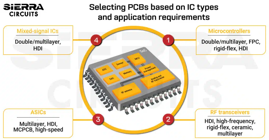
3. PCB selection based on IC types and application requirements
3.1. Microcontrollers (MCUs)
Choosing the right type of circuit board for a microcontroller depends on the MCU’s bit-width (8, 16, or 32), pin count, power consumption, form factor, and the application it serves.

Common boards used for microcontroller integration include:
- Double-layer: Offers more routing flexibility than single-layer boards. It is commonly used with 16-bit MCUs and advanced 8-bit MCUs.
- Multilayer: Ideal for high-pin-count MCUs (32-bit), as it provides better signal integrity.
- Flexible printed circuit (FPC): Used in compact or bendable designs like wearables and medical devices. FPCs are great for mounting CSPs or QFNs.
- Rigid-flex: Combines rigid and flexible sections to handle both structural durability and movement. Perfect for applications like automotive systems or aerospace electronics, where reliability and space optimization are critical.
- High-frequency/low-loss: Critical for radio frequency-enabled MCUs to ensure controlled impedance.
- High-density interconnect (HDI): Enables compact layouts with fine-pitch MCUs like CSP or BGA.
| MCU types | Supported packages | Common PCB types | Example ICs | Applications |
|---|---|---|---|---|
| 8-bit | DIP, SOIC, QFP | Double-layer | ATmega328P, PIC16F877A | DIY projects, toys, and industrial control panels |
| 16-bit | QFP, LQFP, SOIC | Double-layer, multilayer | MSP430, PIC24F | Smart home devices, low-power controllers |
| 32-bit | QFN, BGA, CSP, LQFP | Multilayer, HDI, FPC | STM32H7, ESP32-S3 | IoT, wearables, advanced embedded systems |
| Ultra-low-power | QFN, CSP, UQFN | HDI, FPC | nRF52840, STM32L4 | Fitness trackers, smart sensors |
| RF-enabled | QFN, CSP, BGA | Multilayer, HDI, high-frequency/low-loss | ESP32, CC1310 | BLE devices, Wi-Fi IoT, LoRaWAN nodes, mesh networking |
| Automotive | QFP, BGA | Multilayer, rigid-flex, HDI | NXP S32K, Renesas RH850 | ADAS, ECUs, dashboards |
3.2. System-on-chip (SoC)
SoCs integrate CPUs, GPUs, memory controllers, and peripherals into a single chip. Their PCB requirements are heavily driven by complexity, speed, and form factor.

Standard PCB types employed for SoC IC integration include:
- HDI: Essential for mobiles and embedded SoCs with fine-pitch BGA and CSP packages.
- Multilayer: Commonly used in AI hardware PCBs for integrating artificial intelligence and machine learning (ML) SoCs. These are widely used to support power delivery networks and complex routing of high-speed PCB interfaces like DDR, USB, and PCIe.
- FPC: Enables flexible, lightweight designs for low-pin-count SoCs (CSP/WLCSP) in wearables like smartwatches and medical implants.
- Backplane: Supports modular SoC systems used in data centers or industrial communication systems. For more on boards used in hyperscale servers, see how to design PCBs for data centers and AI servers.
- High-frequency/low-loss: Crucial for system-on-chip ICs handling high-speed data and RF communication in 5G printed circuit boards and mmWave applications.
| SoC types | Supported packages | Common PCB types | Example ICs | Applications |
|---|---|---|---|---|
| Mobile | BGA, FBGA, CSP, WLCSP | HDI, FPC | Apple A15, Snapdragon 8 Gen1 | Smartphones, tablets, wearables |
| Embedded | BGA, QFP | Multilayer | NXP i.MX6, TI Sitara AM335x | Gateways, HMI panels, kiosks |
| AI/ML | BGA | Multilayer, HDI | Google Edge TPU, NVIDIA Jetson Nano | Edge AI, drones, vision systems |
| Networking | BGA | Multilayer, backplane, high-frequency/low-loss | Broadcom BCM2837, Marvell ARMADA | Routers, NAS, industrial servers |
| Automotive | BGA, CBGA | Multilayer, HDI, high-frequency/ low-loss | Tesla HW3, NXP S32V | ADAS, infotainment, ECU systems |
3.3. Power management ICs (PMICs)
Power management ICs regulate, distribute, and convert power efficiently across subsystems. They require boards that ensure efficient heat dissipation, low impedance paths, and EMI compliance.

Commonly used PCB types include:
- Double layer: Used in low dropout regulators (LDOs) and basic battery chargers for simpler power distribution in low-to-medium-complexity designs, balancing performance and cost.
- Multilayer: Enables low-impedance power and ground planes. Isolates analog and digital circuits in mixed-signal PMICs.
- Metal core printed circuit board (MCPCB): Dissipates high thermal loads in power-dense PMICs like LED drivers and motor controllers, which incur significant switching losses.
- High-frequency: Supports high-frequency switching in DC-DC converters by meeting signal integrity and electromagnetic interference (EMI) requirements.
- FPC: Enables close placement of charger ICs to the battery in tight or curved spaces to reduce trace resistance and improve power delivery efficiency.
- HDI: Allows integration of power-dense PMICs with small packages like WLCSPs, CSPs, or QFNs in space-constrained designs.
| PMIC types | Supported packages | Common PCB types | Example ICs | Applications |
|---|---|---|---|---|
| Linear regulator | SOT-23, TO-252, DFN | Double-layer, multilayer | MIC29302, AMS1117, LT1763 | Low-noise analog supplies, sensor biasing |
| DC-DC converter | QFN, LGA, BGA, WLCSP | Multilayer, MCPCB, high-frequency | TI TPS5430, LM22675, MP1584, TPS62840 | Power supply units, embedded boards, LED drivers |
| Integrated PMIC | QFN, BGA, CSP, WLCSP | Multilayer, HDI | Dialog DA9063, TI TPS65982 | Mobile SoCs, tablets, laptops, wearables |
| Battery charger IC | QFN, DFN, SOP, WLCSP | Double-layer, HDI, FPC | BQ24195, MCP73831, MAX17260 | Portable electronics, power banks, wearables |
|
Power sequencer |
QFN, SOIC |
Multilayer, HDI |
TPS3808, LM3880 |
Embedded systems, servers, telecom |
3.4. RF transceivers
RF transceivers handle wireless communication across a range of frequency bands (sub-GHz, 2.4 GHz, mmWave). These ICs require printed boards optimized for low-noise routing and minimal EMI.
Widely used PCB types are:
- HDI: Used for high-density wireless modules like Bluetooth and Wi-Fi, requiring compact parts and close antenna integration on RF boards.
- High-frequency: Essential for sub-GHz and mmWave systems where precise RF trace tuning is critical.
- Rigid-flex: Enables RF module integration with flexible antennas or devices in confined enclosures.
- Ceramic: Preferred for mmWave and RF front-end components due to its excellent dielectric properties and thermal stability.
- Multilayer: Required to isolate analog, RF, and digital planes and integrate shielding and filtering for complex transceiver modules.
| RF transceiver types | Supported packages | Common PCB types | Example ICs | Applications |
|---|---|---|---|---|
| Bluetooth/ Wi-Fi module | QFN, LGA, µBGA | HDI, FPC | ESP8266, CC3200 | IoT devices, wireless peripherals, smart plugs |
| Sub-1 GHz RF | QFN | HDI, high-frequency | CC1101, SX1276 | Industrial IoT, remote sensors, smart meters |
| Cellular modem | LGA, BGA | Multilayer, rigid-flex | SIM7600, Quectel EC25 | GPS trackers, LTE modules, embedded routers |
| RF front-end module | QFN, CSP | High-frequency, ceramic | SKY66112, Qorvo QM12040 | Signal boosters, integrated antenna modules |
| mmWave / 5G transceiver | CBGA, BGA | High-frequency, HDI, ceramic | AD9371, Qualcomm SDX60 | 5G radios, phased arrays, base stations |
3.5. Memory ICs
Memory chips are critical for data storage, buffering, and boot code. The choice of PCBs for IC integration depends on interface speed and density requirements.
PCB types include:
- Double-layer: Adequate for low-speed, low-pin-count memory like electrically erasable programmable read-only memory (EEPROM) and NOR flash.
- Multilayer: Necessary for high-speed dynamic random-access memory (DRAM) and larger address/data bus routing.
- HDI: Used in compact devices with fine-pitch BGA NAND or low-power DDR (LPDDR) memories.
- High-frequency: Maintains signal integrity and timing for high-speed memory interfaces such as DDR (DDR3/ DDR4/DDR5) and graphics double data rate synchronous DRAM (GDDR SDRAM), especially in AI hardware PCBs.
- Backplane: Utilized in server and networking hardware to interconnect memory modules and other components with high-density and long-reach signal paths.
| Memory IC types | Supported packages | Common PCB types | Example ICs | Applications |
|---|---|---|---|---|
| EEPROM | SOIC, TSSOP, SOT-23 | Double-layer | AT24C256, 93C66 | Configuration storage, microcontroller NVM |
| NOR flash | SOP, TSOP, BGA | Double-layer, multilayer | W25Q64JV, S29GL256 | Firmware storage, embedded boot ROM |
| NAND flash | TSOP, BGA | Multilayer, HDI | MT29F4G08, K9F1G08U0D | Mass storage, SSDs, cameras |
| SDRAM/DDR | BGA, FBGA | Multilayer, high-frequency | IS42S32800G, MT41K256M16 | Microprocessor RAM, embedded computing |
| DRAM module | DIMM, SO-DIMM | Multilayer, backplane | DDR4-2400 DIMM, LPDDR5 SO-DIMM | PCs, servers, networking hardware |
3.6. Field-programmable gate arrays (FPGAs)
FPGAs require advanced layouts to support high-speed interfaces, numerous I/O pins, and stable power distribution. The choice of PCBs depends on system complexity, interface needs (PCIe, DDR, high-speed transceivers), and thermal requirements. For more on layout design, see how to design a PCB layout.

Typical PCB types used are:
- Multilayer: Ensures power integrity and dense routing for logic-intensive FPGAs with DDR, PCIe, or SerDes interfaces. Common in AI hardware PCBs, where high data throughput is critical.
- HDI: Required for fine-pitch BGA packaging and high I/O counts in advanced FPGAs.
- High-frequency/low-loss: Maintains signal integrity for high-speed serial transceivers and clocking.
- Backplane: Provides robust, modular interconnects for telecom, data center, or server-based systems.
- Rigid-Flex: Supports high-pin-count FPGA placement on the rigid section with high-speed signals (e.g., SerDes lanes, memory interfaces) routed through flex regions, reducing impedance issues.
| FPGA types | Supported packages | Common PCB types | Example ICs | Applications |
|---|---|---|---|---|
| Entry-level | QFP, TQFP | Multilayer | Lattice iCE40, Xilinx Spartan-6 | Consumer electronics, control logic |
| Mid-range | BGA, QFN | Multilayer, HDI | Intel Cyclone V, Xilinx Artix-7 | Industrial control, embedded vision |
| High-performance | BGA, FBGA | Multilayer, HDI, high-frequency/ low-loss, backplane | Xilinx Kintex UltraScale, Intel Stratix | Data centers, high-speed communication, HPC systems |
| RF-capable | BGA, LGA | Multilayer, high-frequency/low-loss | Xilinx RFSoC, Intel Agilex M-Series | 5G, satellite, software-defined radio |
| Automotive | BGA, CBGA | Multilayer, rigid-flex | Xilinx Zynq UltraScale+, Intel MAX 10 | ADAS, automotive gateways, domain controllers |
3.7. Analog ICs
Analog ICs process continuous signals and are essential in interfacing sensors, actuators, and other analog components with digital systems. They require PCB designs that focus on noise immunity, signal fidelity, grounding, and effective isolation of digital and power circuits.

Frequently used PCB types are:
- Double-layer: Suitable for basic op-amp circuits or sensor signal conditioning with low complexity.
- Multilayer: Ideal for mixed-signal designs where analog and digital sections need isolation.
- HDI: Used in compact analog front-ends or precision analog ICs requiring tight layout tolerances.
- MCPCB: Useful for analog power amplifiers or precision drivers with heat dissipation needs.
| Analog IC types | Supported packages | Common PCB types | Example ICs | Applications |
|---|---|---|---|---|
| Operational amplifiers | SOIC, TSSOP, SOT-23 | Double-layer, Multilayer | LM324, TL072, OPA2134 | Sensor signal conditioning, filters, instrumentation |
| Analog switches/multiplexers | SOIC, QFN | Double-layer, multilayer | CD4051, ADG884 | Data acquisition, audio/video routing, test systems |
| Comparators | SOT-23, SOIC, QFN | Double-layer, HDI | LM339, TLV3201 | Zero-cross detection, over-voltage protection, ADC triggering |
| Analog front-end (AFE) | QFN, BGA, CSP | Multilayer, HDI | ADS1298, ADAS1000 | Biomedical monitoring, industrial sensors, ECG/EEG |
Also see the pros and cons of composite amplifiers for PCB designers.
3.8. LED drivers and lighting ICs
LED driver ICs regulate current or voltage to LEDs for optimal brightness, efficiency, and lifespan. Selecting PCBs for IC integration depends on thermal requirements and EMI compliance.
Common board types for IC integration:
- Double-layer: Suitable for low-power LED drivers with minimal thermal and routing complexity.
- Multilayer: Used for high-power drivers requiring solid ground/power planes for stable power distribution.
- MCPCB: Ideal for high-brightness LED applications needing enhanced heat dissipation. For PCB heat dissipation techniques, see 12 PCB thermal management techniques to reduce PCB heating.
- HDI: Preferred for compact, high-density LED drivers with small package ICs like QFN.
- Rigid-flex: Required in automotive and rugged lighting systems needing shock resistance and mechanical durability.
| LED driver types | Supported packages | Common PCB types | Example ICs | Applications |
|---|---|---|---|---|
| Linear | TO-220, SOT-223 | Double-layer | NSI45020, AMC7135, CAT4101 | Indicator lights, low-power lighting |
| Switching | QFN, D²PAK | Multilayer, MCPCB, HDI | MAX16832, TPS92692-Q1 | High-brightness LEDs, automotive lighting |
| Backlighting | QFN, SOIC | Multilayer, HDI | LT3477, AL8805 | Display backlighting, signage |
| Automotive | QFN, TSSOP | Multilayer, MCPCB, rigid-flex | TPS92630-Q1, NCV78763 | Automotive headlamps, tail lights |
3.9. Application-specific integrated circuits (ASICs)
ASICs are custom-designed chips built for a specific function, such as image processing, neural network acceleration, cryptocurrency mining, and power management in mobile devices.
Boards for integrating these ICs must meet stringent requirements of power delivery and thermal dissipation due to the high-density nature of these chips.
Common board types include:
- Multilayer: Enables complex routing and dedicated power and ground planes essential for integrating ASICs.
- HDI: Enables HDI routing to support ASICs with high pin counts and fine-pitch BGAs in mobile chipsets.
- MCPCB: Offers better heat dissipation for power-intensive ASICs used in telecom/data center power systems and EV inverters.
- High-speed: Ensures signal integrity and EMI control in ASICs for SERDES, PHYs, or high-frequency data links.
| ASIC types | Supported packages | Common PCB types | Example ICs | Applications |
|---|---|---|---|---|
| Logic | BGA, QFN, WLCSP, QFP | Multilayer, HDI | Apple A16 Bionic, Google TPU, NVIDIA Tegra X1 | Smartphones, data center AI, edge computing, telecom infrastructure |
| Power | BGA, QFN, LGA | MCPCB, multilayer | TI TPS65987, Qualcomm PM8150, ADI ADP5054 | Power supplies, EVs, battery management, data centers |
| Communication | BGA, CBGA, FCBGA, QFN | Multilayer, HDI, high-speed | Broadcom BCM56980, Qualcomm QTM545, Marvell 88E6390 | 5G, Wi-Fi, Ethernet switches, automotive radar |
| Mixed-signal | QFN, BGA, TSSOP, WLCSP | Multilayer, HDI | Cirrus Logic CS4272, ADI AD9361, TI ADS1298 | Professional audio systems, medical imaging, SDR, automotive sensors |
3.10. Sensors ICs
Sensors convert physical phenomena into electrical signals. They require boards that support clean analog routing and noise reduction.
Common PCB types for IC integration:
- Single-layer: Used for basic analog sensors with low power and straightforward signal paths.
- Double-layer: Common for sensors requiring moderate complexity and mixed analog/digital signals (e.g., ADC-integrated pressure or humidity sensors).
- Multilayer: Ideal for high-resolution or multiple output sensors (e.g., image sensors, IMUs) to support complex interfaces and noise isolation.
- HDI PCB: Used for modern sensors (e.g., MEMS, biosensors) in fine-pitch packages with multiple interfaces (e.g., SPI, I²C, analog out, interrupts, power rails), requiring dense routing in compact layouts.
- Rigid-flex: Utilized in wearables, automotive, and medical devices, where sensors are placed on movable sections.
| Sensor IC types | Supported Packages | Common PCB Types | Example ICs | Applications |
|---|---|---|---|---|
| Temperature | SOT-23, SOIC, DFN | Single-layer, double-layer | LM35, TMP36 | Thermostats, automotive climate control |
| Proximity | QFN, SOIC, LGA, WLCSP | Double-layer, HDI | APDS-9960, VCNL4040 | Object detection, industrial robots |
| Motion | LGA, QFN, DFN | Multilayer, double-layer | AS3935, ADXL345, MPU6050 | Security systems, wearables, motion tracking |
| Humidity and pressure | LGA, QFN, DFN | Double-layer, multilayer | BME280, MPL3115A2 | Weather stations, environmental monitoring, smart homes |
| Gas | LGA, QFN, DFN | Double-layer, rigid-flex | SGP30, CCS811, BME688 | Air quality monitoring, gas leak detection |
3.11. Mixed-signal ICs
Mixed-signal ICs integrate both analog and digital circuits on a single chip. PCBs for these ICs should be designed to minimize noise and preserve signal integrity across the analog and digital domains.

Widely used PCB types are:
- Double-layer: Suitable for simpler designs that require isolation of analog and digital traces.
- Multilayer: Preferred for separating analog/digital ground planes, reducing EMI, and improving routing flexibility.
- HDI: Enables compact, low-inductance routing for DACs, PLLs, and audio codecs with fine-pitch packages, minimizing crosstalk in audio and communication systems.
- High-frequency: Required for high-speed ADCs (e.g., >500 MSPS) to ensure signal integrity, controlled impedance, and low-jitter clocking in RF and data acquisition systems.
| Mixed-signal IC types | Supported packages | Common PCB types | Example ICs | Applications |
|---|---|---|---|---|
| Analog-to-digital converter (ADC) | SOIC, QFN, BGA, TSSOP | Double-layer, multilayer, high-frequency | ADS1115, AD9246, MCP3008 | Data acquisition, measurement systems, medical devices, IoT |
| Digital-to-analog converter (DAC) | MSOP, QFN, SOIC, TSSOP, CSP | Double-layer, multilayer, HDI | MCP4921, AD5686 | Audio processing, waveform generation, motor control |
| Phase-locked loop (PLL) | SOIC, QFN, TSSOP | Multilayer, HDI, high-frequency | CDCE913, LMX2594 | Clock generation, signal synchronization, RF synthesis, networking |
| Audio codec | QFN, TQFP, BGA | Multilayer, HDI | CS4272, TLV320AIC3204 | Audio interfaces, communication systems, automotive infotainment |
3.12. Image sensors
Image sensors are highly sensitive analog-digital components that require compact and low-noise PCBs.
Commonly used board types include:
- HDI: Best suits for fine-pitch, small-footprint sensors like CMOS sensors in phones or drones.
- FPC: Ideal for camera modules in mobile and embedded applications where the sensor is mounted separately.
- Multilayer: Supports power distribution, image signal processor (ISP) integration, and EMI shielding.
- Rigid-flex: Well-suited for rugged imaging systems, wearables, or automotive cameras.
- High-frequency/low-loss: Maintains signal integrity when transferring high-speed pixel data over MIPI CSI or LVDS interfaces.
| Image sensor types | Supported packages | Common PCB types | Example ICs | Applications |
|---|---|---|---|---|
| CMOS | COB, CSP, WLCSP, BGA | HDI, FPC | Sony IMX586, OV2640 | Smartphones, drones, webcams |
| CCD | LCC, DIP, ceramic | Multilayer | Sony ICX285AL, KAI-2020 | Medical imaging, scientific cameras |
| Automotive | CSP, FCBGA | Rigid-flex, HDI, high-frequency/low-loss | ON Semi AR0144, Sony IMX490 | ADAS, surround view cameras |
| 3D | LGA, BGA | Multilayer, HDI, high-frequency/low-loss | Sony IMX556, OV9282, IMX570 | Robotics, AR/VR, gesture control, 3D scanning |
3.13. RF amplifiers
High-frequency radio frequency amplifiers, such as low-noise amplifiers (LNAs), require specialized RF PCB materials and layout techniques to minimize signal loss, crosstalk, and noise.

The selection of PCBs for IC integration is driven by RF performance, thermal characteristics, and layout constraints.
Frequently used printed board types for RF amplifier IC integration are:
- High-frequency/low-loss: Uses PTFE-based laminates like Rogers RO3003 to maintain low insertion loss and impedance control in RF ICs at GHz frequencies.
- Multilayer: Supports power isolation, ground referencing, and filtering in RF front-end modules.
- HDI: Enables tight RF routing in compact modules using fine-pitch QFN or LGA packages (<0.5 mm), common in mobile, Wi-Fi, and 5G RF amplifiers.
- Rigid-flex: Supports mechanically constrained RF front-end modules for systems like drones, V2X, and tactical radios where vibration resistance and compact, connector-less routing are critical.
- MCPCB: Used in high-power RF amplifiers (e.g., base stations, radar) for thermal dissipation.
| RF amplifier types | Supported packages | Common PCB types | Example ICs | Applications |
|---|---|---|---|---|
| LNA | SOT-23, QFN, DFN | High-frequency/ low-loss, HDI | Skyworks SKY67151, Infineon BGA2851 | Wi-Fi front-ends, GPS modules, satellite receivers |
| Power | QFN, LGA, TO-39 | MCPCB, multilayer, High-frequency/low-loss | Wolfspeed CGHV96100F, NXP MRFE6VP61K25H | Base stations, RF transmitters, radar |
| Broadband | SOT-89, QFN | Multilayer, high-frequency/ low-loss | Analog Devices ADL5610, MACOM MAAM-011100 | Test equipment, RF instrumentation |
| Automotive | QFN, DFN | High-frequency/ low-loss, rigid-flex | NXP BGU7258, NXP BGU7258Q, Infineon BGA7H1N6, | Vehicle radar, automotive connectivity |
To learn how to design radio-frequency PCBs with signal integrity, see 9 factors that impact RF PCB design and tips to resolve them.
3.14. High-speed transceivers
High-speed transceivers handle data rates from hundreds of Mbps to multiple Gbps, demanding strict PCBs with EMI compliance.

Commonly used PCBs for microchips are:
- High-frequency/low-loss: Required for maintaining signal quality over high-speed serial interfaces like PCIe, USB 3.x, HDMI, or SerDes.
- Multilayer: Offers dedicated ground and power planes with reduced signal noise, essential for high-speed differential pairs used by transceiver ICs.
- HDI: Enables tight trace geometry and via-in-pad designs without crosstalk, essential for gigabit-speed transceivers.
- Backplane: Supports pluggable high-speed transceiver modules in networking gear.
| Transceiver types | Supported packages | Common PCB types | Example ICs | Applications |
|---|---|---|---|---|
| USB 3.x / PCIe | QFN, BGA | Multilayer, HDI | TI TUSB1046, Diodes Inc. PI3EQX12908 | Laptops, embedded systems, external interfaces, docking stations |
| SerDes | BGA, CSP | HDI, high-frequency/low-loss | TI DS90UB954, Maxim MAX96717 | Automotive cameras, industrial vision, displays, ADAS, infotainment |
| Fiber optic | LGA, BGA | Multilayer, backplane | Broadcom BCM84790, Finisar FTLF8536P4BCL | Data centers, optical communication switches, telecom |
| Ethernet PHYs (1G/10G) | QFN, BGA | High-frequency/ low-loss, multilayer | Marvell 88E1512, Intel i210-AT, Marvell 88E1512 | Networking switches, routers, industrial Ethernet, IoT devices |
Download our handbook to learn how to design a manufacturable board without board respins.

Design for Manufacturing Handbook
11 Chapters - 96 Pages - 90 Minute ReadWhat's Inside:
- Annular rings: avoid drill breakouts
- Vias: optimize your design
- Trace width and space: follow the best practices
- Solder mask and silkscreen: get the must-knows
Download Now
4. 8 essential DFA guidelines for PCB chip integration
- Check for part availability and obsolescence early in the design process
- Use standard, widely available ICs to reduce cost and simplify the supply chain. Component availability and lifecycle must be verified during design to ensure all BOM parts are readily available.
- Avoid using obsolete or end-of-life ICs that could disrupt assembly or delay production. To eliminate potential supply chain disruptions, opt for component management services offered by your fabricator.

Lifecycle of electronic components.

- Consider thermal and mechanical aspects of parts to maintain solder joint integrity
- Ensure all chip components can withstand mechanical forces during automated assembly (e.g., vibration or component placement pressure). Standardized packages (SOIC, QFN, BGA, and TSSOP) are compatible with automated assembly processes.
- Place large QFP, QFN, BGA, or PoP packages along the horizontal direction of the assembly line to minimize the effects of bow and twist. This ensures total board warpage remains within the 0.75% tolerance for SMD-mounted assemblies.

Recommended IC position on PCBs to minimize stress due to warpage. - For socketed chips (e.g., FPGAs, MCUs), position sockets away from sensitive packages to avoid mechanical stress during repeated plug/unplug cycles.
- Avoid using fasteners when possible. Instead, use surface-mount packages with integrated heat sinks to reduce cost and complexity.
- Maintain optimum component clearances to prevent tombstoning and solder bridging
- Adhere to component spacing as per IPC-2221 or specific assembly requirements to prevent soldering defects.
- Define a minimum placement courtyard around chip components (including package body and land pattern) to ensure sufficient spacing for assembly and rework.
Follow these clearance guidelines for chip integration:
-
-
- 0.25 mm for standard chips unless otherwise specified.
- 1 mm for BGA devices to facilitate inspection and rework.
- 0.15 mm for very small packages (e.g., <0603) to ensure reliable placement.
- 0.5 mm for crystals and canned capacitors.
- 1.27 mm (50 mil) for connectors.
-

This courtyard zone is especially critical for complex ICs like BGAs and QFNs, which require additional clearance for rework and inspection access.
-
- Ensure a minimum 8 mil spacing between the edge of the component pad and the hole wall. For manual soldering, this ranges between 50 to 100 mil.

Maintain a minimum of 8 mil part-to-hole spacing. - Maintain a minimum spacing of 7 mil between the component pad’s edge and the edge of the annular ring. However, this can be between 50 and 100 mil for manual soldering.

Maintain a minimum of 7 mil IC to annular ring spacing on your PCB. - Keep appropriate edge clearance for depanelization. The recommended clearance between the part and the board edge is as follows:
- Larger components (BGA, QFP, DIP, and PLCC): 125 mil
- Smaller components (SOT-23, DFN, QFN, TSSOP, and SOIC): 25 mil
- Manually installed components: 10 mil
- Ensure a minimum 8 mil spacing between the edge of the component pad and the hole wall. For manual soldering, this ranges between 50 to 100 mil.

For more, see component placement guidelines for PCB design and assembly.
- Optimize PCB layout for soldering efficiency and reliable joint formation
- Prefer SMT components over through-hole for chip integration due to compatibility with automated reflow soldering and efficient mass production.

Soldering techniques used for through-hole and SMT components. - Consider placing BGA and other surface-mount ICs on only one side of the board to enable a single reflow soldering process, followed by the mounting of through-hole components with wave soldering or manual soldering. This helps avoid double-sided assembly and reduces flipping and alignment costs.

Standard SMD clearance requirements on a PCB. - Align ICs perpendicular to the solder wave to prevent solder bridging caused by membrane formation between closely spaced leads.
- Rotate QFPs or similar ICs with leads on all four sides by 45 degrees relative to the wave. This distributes the solder flow evenly across all sides and prevents bridging at corners.

Orient ICs perpendicular to the solder wave direction and rotate QFPs by 45° to improve the solder joint quality. - Avoid long leads and oversized pads on ICs to prevent excess solder accumulation and bridging during wave soldering.
- Provide adequate clearance between pads to avoid solder bridging during reflow. Ensure sufficient space for manual soldering, inspection, and potential rework operations in densely populated areas.

Make sure there is sufficient spacing between the components for manual soldering and rework.
- Prefer SMT components over through-hole for chip integration due to compatibility with automated reflow soldering and efficient mass production.
For THT design considerations, see through-hole assembly design rules.
- Design for automated pick-and-place efficiency
- Select components with tight dimensional tolerances for reliable automated placement. Snap-fit, self-aligning, or self-locating chip components streamline automation.

Sierra Circuits’ assembly expert working on a Juki pick-and-place machine. - Choose chip packages that are easy to orient during assembly to reduce reorientation steps. Minimize angular component orientations to simplify the pick-and-place process. Some automated machines may require additional setup time for rotated components.
- Design with precise component footprints, clear fiducials, and optimal pad geometry to support robotic-assisted SMT placement necessary for high-pin-count or high-speed ICs like DDR5, AI processors, and LiDAR chips, where even slight misalignment causes signal interference.
- Select IC packages with clear pin 1 markings and symmetrical shapes to ensure easy orientation during automated pick-and-place. Minimize angular orientations to reduce setup time and placement errors
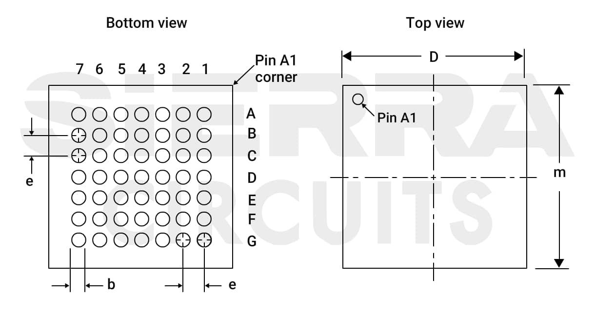
Pin 1 marking on a BGA using a circle.
- Select components with tight dimensional tolerances for reliable automated placement. Snap-fit, self-aligning, or self-locating chip components streamline automation.

For more, read PCB design for assembly checklist.
- Ensure the layout supports testing and adheres to standards
- Include adequate spacing around critical components to allow for automated inspection methods such as AOI and X-ray.

Recommended pad-to-pad spacing for common IC packages to ensure soldering quality and facilitate inspection. - Add fiducial marks at the board’s edge:
- Diameter: 1–3 mm
- Spacing: 3 mm from the board’s edge
- 3 global fiducials for board alignment.
- 2 local fiducials (diagonally) on the outside of the quad-packaged SMT component to recognize their footprint.

3 global and 2 local fiducial markers are placed on the board.
- Place BGA and other leadless packages (e.g., QFN) on only one side of the PCB to simplify assembly and inspection. If dual-side placement is unavoidable, avoid aligning them on the same XY coordinates on both sides to prevent complications during X-ray inspection and rework.
- Implement boundary scan (joint test action group or JTAG) for digital ICs, processors, and FPGAs where physical probing is impractical.
- Design ICs like microcontrollers or SoCs with built-in self-test (BIST) features to self-verify internal logic and perform startup diagnostics, detecting defects early to reduce rework costs and enhance reliability.
- Follow IPC -6012 standards for chip-level assembly quality.
- Match IPC class 2 or 3 based on application criticality (e.g., class 3 for aerospace and military).
- Include adequate spacing around critical components to allow for automated inspection methods such as AOI and X-ray.
- Refine your BOM to reduce the overall cost
- Reduce chip/component count by combining or eliminating redundant parts to simplify assembly.
- Avoid using non-washable memory ICs and other unsealed components, as they require manual insertion after cleaning, increasing assembly time and expense.
- Select RoHS-compliant ICs to simplify integration, ensure regulatory compliance, and avoid costly reballing or hybrid assembly processes when integrating components like BGAs on PCBs.
- Do not include (DNI) chips should be clearly marked in the BOM and managed for printed board prototypes or future upgrades.
To learn how to design a prototype, see building a PCB prototype from scratch.
- Verify footprint and pad dimensions for accurate chip placement
- Refer to the component datasheets and follow industry standards such as IPC-7351 when creating footprints.
- Ensure MPNs exactly match manufacturer-recommended footprints to prevent mismatches during chip placement.
- Confirm that footprint outlines align with actual chip dimensions for reliable automated placement.
- Verify correct pad sizes. Undersized pads can lead to poor solder joints, whereas oversized pads can cause chips to float during reflow.
During a routine DFA check of a circuit board design provided by a customer, our PCB assembly engineers discovered a footprint mismatch. The mechanical dimensions of multiple components (U1, U2, U3, U12, and U14 ) in the Gerber did not match the datasheet.
The Gerber files indicated a pad footprint intended for a significantly larger package, whereas the actual component, an MSOP-8 package op-amp (AD8655ARMZ-REEL), was much smaller. This inconsistency raised concerns about potential soldering issues, weak joints, and possible open circuits during assembly.

We immediately initiated a thorough review of the design files and collaborated with the client, who confirmed the mismatch and provided a compatible replacement in a SOIC-8 package (Digi-Key PN: AD8655ARZ-REEL7CT-ND).
The proactive detection and resolution of the footprint mismatch avoided potential assembly errors, associated costs, and production delays.
Sierra Circuits performs a thorough DFA analysis to ensure error-free PCBAs. To learn more, see our PCB assembly capabilities.
5. 5 DFM rules for integrating ICs into printed boards
- Implement adequate thermal relief for reliable chip soldering
- Ensure proper thermal relief in power/ground pads under the chip (e.g., exposed pad on QFN) to avoid starved thermal relief conditions that lead to poor solder joints.

Starved thermals can affect the soldering process.
- Ensure proper thermal relief in power/ground pads under the chip (e.g., exposed pad on QFN) to avoid starved thermal relief conditions that lead to poor solder joints.
Thermal spokes help retain heat during reflow, enabling proper solder joint formation.

- Ensure reliable solder mask alignment to avoid open circuits
- Maintain proper solder mask registration by controlling its opening and expansion to prevent partial pad exposure or misalignment during curing.

Solder mask registration defect. - Provide at least 1.6 mil pad-to-solder mask edge clearance around fine-pitch pins (e.g., BGA, QFN) to prevent solder bridging during reflow.

Maintain a 1.6 mil of solder mask clearance between the pad and mask edges. - Design solder mask dam ≥4 mil between solderable surface features to ensure reliable isolation.

Have a minimum 4 mil of solder dam to avoid solder bridges.
- Maintain proper solder mask registration by controlling its opening and expansion to prevent partial pad exposure or misalignment during curing.
- Maintain via and pad integrity for reliable chip integration
- Ensure vias connected to chip nets have sufficient annular ring size to support reliable plating and long-term connection integrity. An insufficient annular ring results in an open circuit.
- Maintain a minimum 10 mil clearance between annular rings and adjacent copper pads to prevent shorts during chip mounting in high-density layouts.

Improper annular ring clearance can cause shorts in voltage planes. - Avoid annular ring breakouts under chips. This occurs when the drill hole is too close to or breaks through the copper pad, reducing the effective pad area and increasing the risk of open circuits or weak solder joints. For more on PCB drilling, see the dos and don’ts of PCB drilling.

Cross-sectional view of an annular ring with the hole drilled slightly off-center.
-
- Maintain at least 10 mil clearance between non-plated holes (NPH) and copper features to prevent unintentional damage to copper traces or pads connected to IC power or signal pins.
- Prevent tangency of annular rings, where the copper ring around the hole touches adjacent features, as this can cause electrical shorts and reduce manufacturing yield, especially in via-in-pad designs.

Tangency can cause connection problems between the via and the copper features - Keep via aspect ratios 10:1 for through-holes and 0.8:1 for microvias to prevent plating defects. This is essential to ensure plating consistency in high-density via structures under or near chips, as higher aspect ratios make it more difficult to achieve reliable copper plating inside the vias.
- Ensure proper drill-to-copper clearance near chip areas to accommodate fabrication tolerances and prevent shorts. Stick to these guidelines:
- 1-layer (laser): Minimum 5 mil; preferred 6 mil
- ≤6 layers: Minimum 6.5 mil; preferred 8 mil
- 8 layers: Minimum 7 mil; preferred 10 mil
-
- Use via-in-pad, which accommodates tighter component pitch sizes (like 0.5 mm) and helps reduce the PCB’s overall size. This technology is ideal for the BGA footprint components.
- Follow the best high-speed routing practices to avoid signal degradation
- Design trace widths and spacing to support controlled impedance, particularly for DDR, USB, PCIe, and similar PCB interfaces.
- Stick to the spacing rules for flashover prevention based on copper weight (e.g., ≥7 mil for 2 oz copper).
Table 18: Minimum recommended spacing between conductors and line width based on copper thickness Start copper Outer layers Inner layers Min. line width (mil) Min. spacing (mil) Min. line width (mil) Min. spacing (mil) 5 microns 2 3 2 2 9 microns 3 3 2.5 2.5 1/2 oz 4 3.5 3 3.25 1 oz 5 5 4 4.25 2 oz 7 7 6 6.25 3 oz 11 11 7 8 4 oz 14 14 8 10 5 oz 16 16 9 11 6 oz 20 20 10 12
-
- Remove stubbed or unconnected traces from chip nets, especially differential pairs, to prevent signal reflections.
- Ensure sufficient spacing between internal traces and chip pins to avoid unintentional shorts.
For more high-speed routing guidelines, see 11 best high-speed PCB routing practices.
- Validate fabrication and assembly clearances to ensure manufacturability
-
- Follow your fabricator’s minimum specifications, including trace width, trace spacing, via size, pad size, etc.
- Use DFM rule checks in CAD tools to catch violations early.
- Maintain at least 20 mil clearance from V-score lines and 10 mil from mouse bites to copper pads used for IC mounting to prevent mechanical damage during depanelization.

Keep copper pads at least 20 mil away from V-score lines to avoid damage during depanelization. - Avoid silkscreen on chip pads, as it can interfere with solder paste deposition or chip placement. Maintain standard silkscreen spacing:
- Silkscreen-to-pad: 4.5 mil
- Silkscreen-to-copper: 6 mil
- Silkscreen-to-hole spacing: 8 mil
- Keep copper pours away from board edges, especially if chips are placed near boundaries, to avoid delamination or damage during depanelization. Ensure copper-to-board edge spacing complies with mechanical clearance requirements.
- Board edge to nearest copper feature clearance (inner planes): 15 mil
- Board edge to nearest copper feature clearance (outer planes): 10 mil

Provide all necessary DFM-related files to your board fabricator and assembler to support accurate chip-level manufacturing, inspection, and assembly. These include Gerber/ODB++ files/IPC-2581, NC Drill files, IPC-356A netlist, pick-and-place files, and detailed fabrication/assembly notes (in PDF format).
Key takeaways:
- Chip architectures like x86, ARM, RISC-V, GPU, and ASIC have distinct applications and board needs.
- Ensure precise RF trace tuning by using high-frequency PCBs for RF transceivers, especially in sub-GHz and mmWave systems.
- Isolate analog signals and reduce noise by designing with multilayer or HDI printed boards that provide clean grounding and layout for analog ICs.
- Manage heat and EMI by selecting MCPCB, multilayer, or rigid-flex boards tailored for high-current lighting applications using LED driver ICs.
- Optimize performance and miniaturization by integrating ASICs on multilayer or HDI boards with robust thermal and signal handling.
- Enable precision and compact integration by using HDI, rigid-flex, or multilayer PCBs with controlled analog routing for sensor ICs.
- Isolate analog and digital domains effectively by designing with multilayer or HDI printed boards that manage crosstalk and grounding for mixed-signal ICs.
- Facilitate high-speed data transmission and tight form factors by choosing HDI, FPC, or rigid-flex printed circuit boards for communication ICs.
The type of printed circuit board used directly impacts a chip’s performance, efficiency, and reliability. With advancements in microchip technology, selecting the right PCBs for IC integration becomes crucial to achieve the desired thermal performance and signal integrity.
Have questions about printed circuit boards? Post your queries on SierraConnect. Our PCB experts will answer them.

About Pooja Mitra : Pooja Mitra is an electronics and communication engineer. With an experience of over three years in the PCB industry, she creates industry-focused articles that help electrical and PCB layout engineers.


Start the discussion at sierraconnect.protoexpress.com