Contents

On-demand webinar
How Good is My Shield? An Introduction to Transfer Impedance and Shielding Effectiveness
by Karen Burnham
Here’s a PCB design for assembly checklist you can refer to before you proceed with the assembly process. This includes key considerations such as footprint design, component placement, soldering considerations, solder mask checks, BOM assessment, testing, and panelization.
By integrating these DFA checks into your design workflow, you can optimize your layout designs and ensure a streamlined assembly process, reduced costs, and superior board quality.
Highlights:
- Footprint design: Component footprints should align precisely with the datasheet measurements to prevent dimensional discrepancies
- Bill of materials: Verify part numbers, descriptions, and manufacturer details in the BOM
- Component placement and spacing: Isolate components by functionality to prevent signal interference and enhance performance. Maintain optimum spacing between components and other PCB features for optimal layout
- Solder mask clearances: Implement correct solder mask clearances to prevent unwanted pad overlaps and shorts
- Silkscreen text: Ensure reference designators are legible
- Test points and probing: Include test probes near component legs for efficient testing and troubleshooting
- Panelization: Orient boards consistently, add alignment marks, and avoid V-scoring near components during panelization for smoother production
What can go wrong if you overlook the DFA rules?
Ignoring DFA rules makes your board harder to assemble, increases the risk of errors, and impacts long-term reliability.
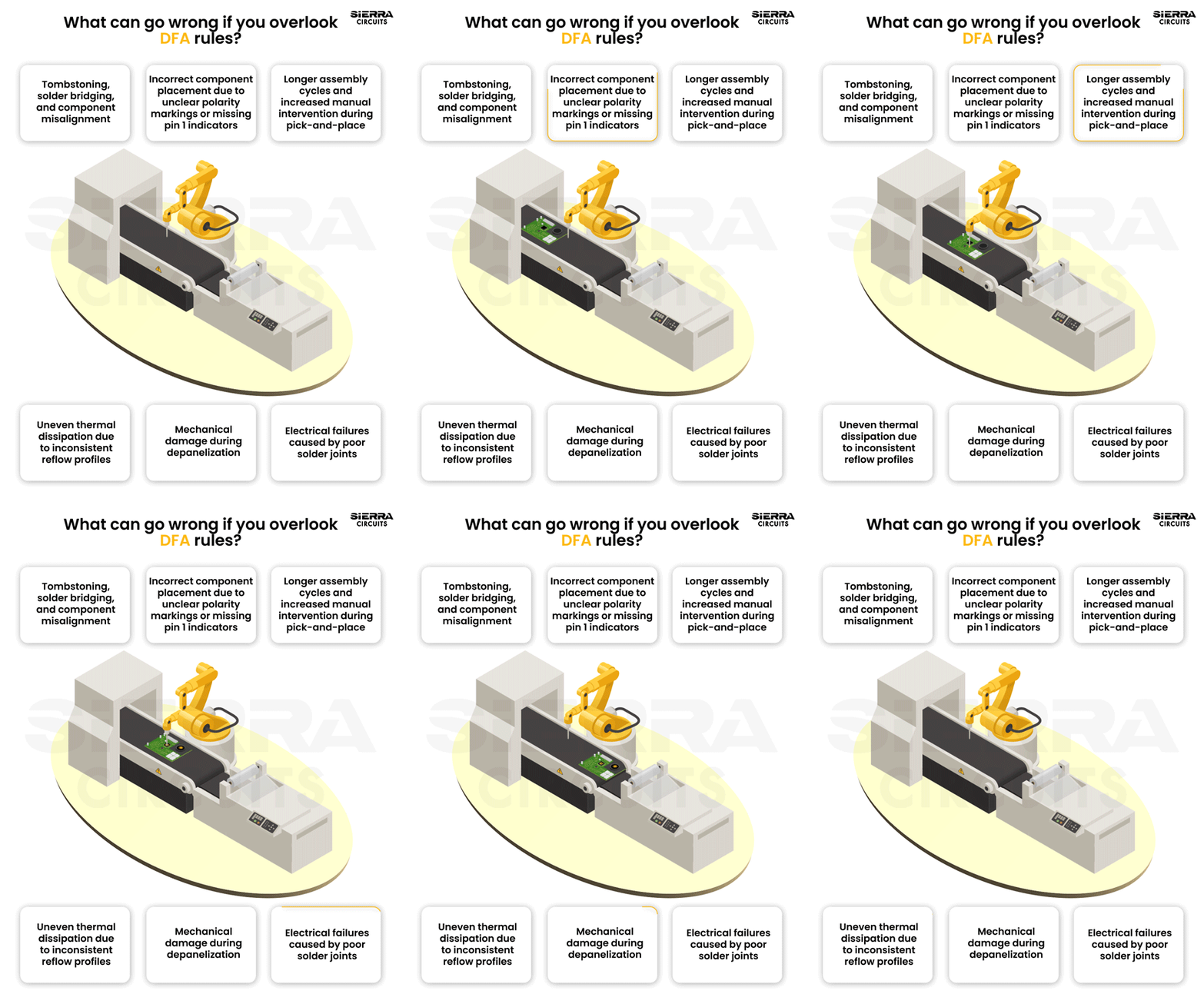
Defects such as tombstoning, solder bridging, component misalignment, and wrong polarity markings are among the most common challenges faced during assembly. These problems can directly affect functionality, especially in dense or fine-pitch layouts.
Tombstoning typically occurs when uneven wetting forces lift one end of a passive component, often due to imbalanced thermal profiles or inconsistent pad design.
Solder bridging, on the other hand, creates unintended electrical connections between adjacent pads, usually resulting from excessive solder paste or improper stencil design.
Component misalignment further complicates assembly, as even slight positional errors during placement can lead to functional issues or reduced reliability, especially in high-density or fine-pitch designs.
Unclear or inconsistent polarity markings significantly increase the risk of incorrect part placement, particularly for diodes, capacitors, and ICs. When markings on the silkscreen or component body are ambiguous, operators and automated systems may misinterpret orientation. This issue becomes more pronounced in high-volume environments.

It can also impact the pick-and-place process and slow down production cycles. Component placement disruptions not only increase assembly time but also introduce variability in quality.
In addition, poor solder joints caused by insufficient wetting, voids, or improper temperature control can lead to intermittent or permanent electrical failures.
Such defects are often difficult to detect during initial inspection and may only surface during field operation, impacting product reliability and customer trust.
Failing to follow DFA rules can lead to insufficient spacing between components, increasing the risk of damage during depanelization. When components are placed too close to board edges or breakaway tabs, separation can introduce mechanical stress, resulting in cracked solder joints or damaged parts.
In addition, inconsistent reflow profiles can cause uneven heat distribution, leading to hotspots or incomplete soldering. These thermal imbalances not only weaken joint quality but can also degrade component performance over time, particularly in thermally sensitive applications.
To learn how to structure a perfect assembly data package, watch our webinar: what your CM wishes you knew about design for assembly.
9 design for assembly checks PCB layout engineers should perform
The checklist helps you identify potential assembly issues early, ensuring higher yield, reduced rework, and a smoother transition from design to production.
1. Ensure accurate alignment between the footprint and physical dimensions of the component

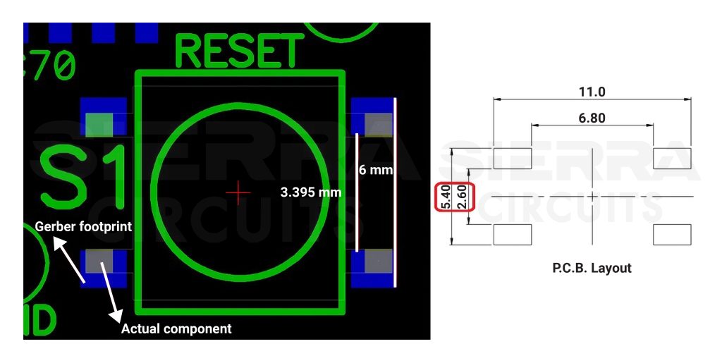
- Footprints must accurately match the physical dimensions of the component given in the datasheet. The image below shows the dimensions of a component in the layout (left) and the datasheet (right). You can see that the dimensions in the layout and the datasheet do not match. Always verify the footprints with the datasheet.
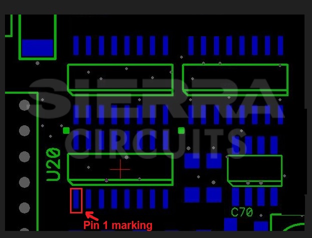
- Clearly indicate the polarity and pin 1 marking to ensure correct component orientation.
- Verify if pad sizes and shapes align with the component’s lead.
- Ensure the footprint matches the most recent version of the component datasheet provided by the manufacturer.
2. Define fiducial markings in the assembly drawing for an effective soldering process
- Define PCB assembly instructions for the top and bottom board layers.
- Make sure the part outline is aligned with the pick and place files.
- Incorporate individual components’ reference designators and pin 1 marking.
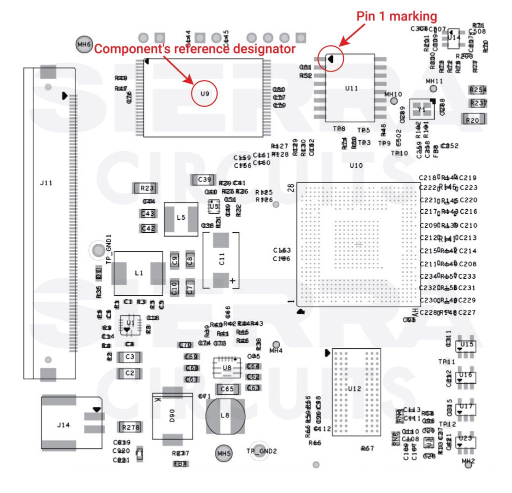
- Mention any unique handling needs for critical components such as ESD devices, heatsinks, and connectors.
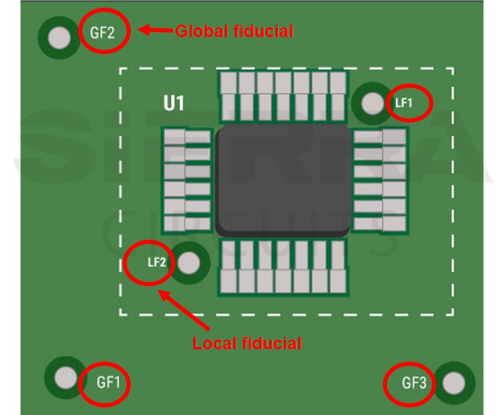
- Implement fiducial marks using a circular non-drilled copper layer without a solder mask on both the pad and stencil.
- The mark should be 40 to 118 mil in diameter.
- Clearance between the fiducial and edge should be 118 mil.
- Place three global fiducials at the board’s edge and two local fiducials diagonally on the outside of the component, where GF1, GF2, and GF3 are global fiducial markers, and LF1 and LF2 are local fiducial markers in the image below:
For more, download the Design for Assembly Handbook.

Design for Assembly Handbook
6 Chapters - 50 Pages - 70 Minute ReadWhat's Inside:
- Recommended layout for components
- Common PCB assembly defects
- Factors that impact the cost of the PCB assembly, including:
- Component packages
- Board assembly volumes
Download Now
3. Verify component MPN in the BOM
Having a clean BOM is an integral part of the design for assembly checklist.
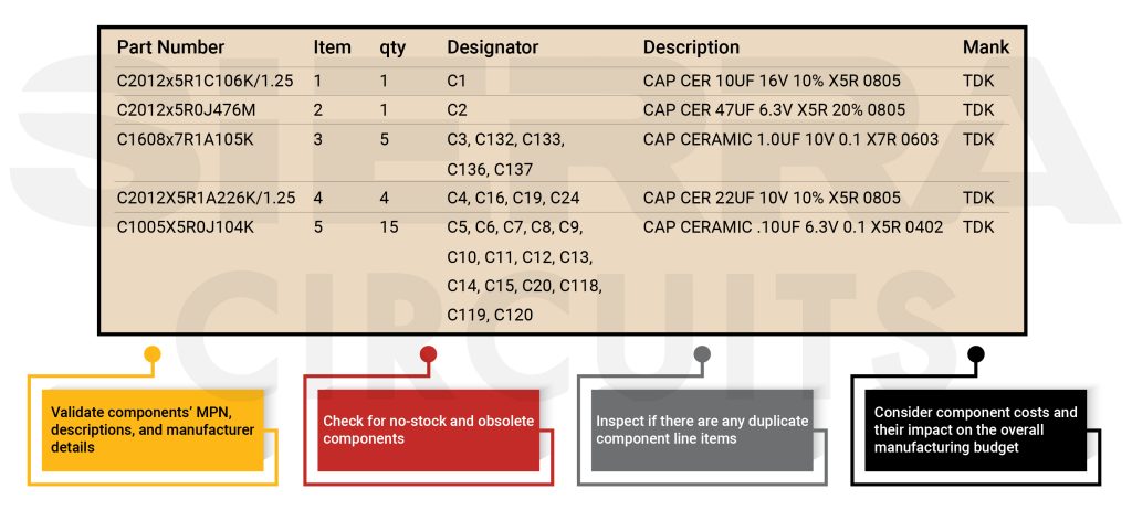
- Validate part numbers, descriptions, and manufacturer details.
- Verify components listed in the BOM are readily available and have reasonable lead times to avoid production delays.
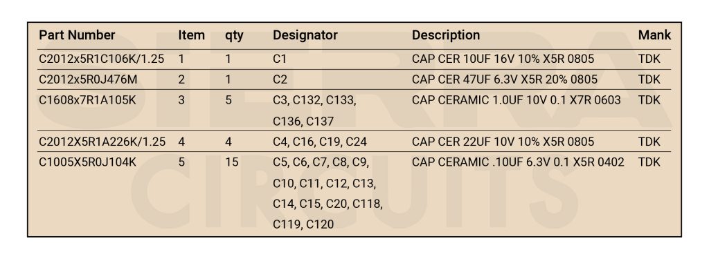
- If there are any obsolete components in your component list, identify the viable alternatives, especially for critical parts.
- For consigned assemblies, adhere to your CM’s kitting guidelines to avoid part shortages.
- Inspect if there are any duplicate component line items.
- Consider component costs and their impact on the overall manufacturing budget.
Are you worried about sourcing low-quality/counterfeit components, price inflation, and inefficient inventory management? We got you covered. Sierra Circuits’ customer-owned inventory services (COIN) is a personalized component sourcing and stocking program designed to meet your specific needs.
With COIN, we procure and store the required parts for your PCBAs, eliminating the risk of counterfeit or low-quality components while ensuring you have access to the necessary parts when you need them.
See our FAQs on COIN services.
4. Isolate the components to avoid signal interference
- Isolate the components based on their functionalities, for instance, RF, motor control, and filter circuits.
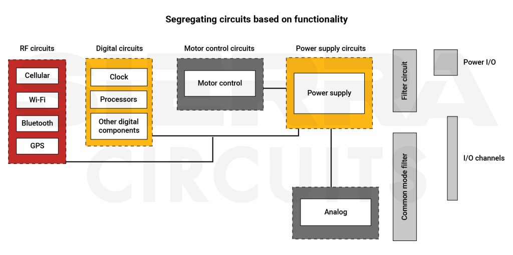
- Separate analog and digital components to avoid signal interference.
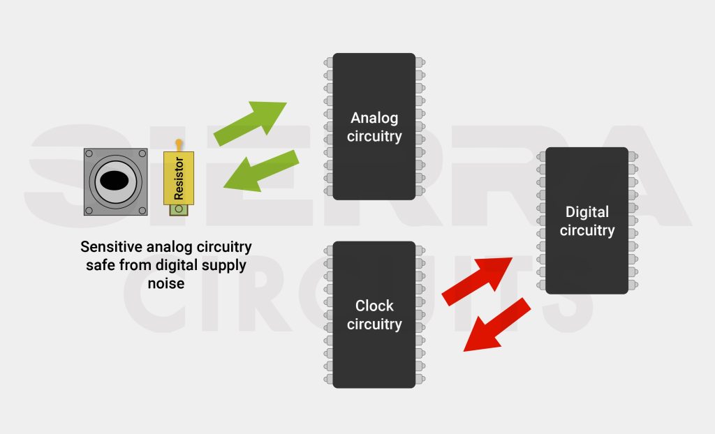
- It’s important to analyze voltage and current levels. Group the circuits with similar VCC and GND connections and position them in close proximity to one another.
5. Provide optimum component-to-component and part-to-copper feature clearances
5.1 Part-to-part spacing
- Incorporate the passive component land pattern-chip (resistor, capacitor, and inductor) clearances as mentioned in the table below (all values are in mil):
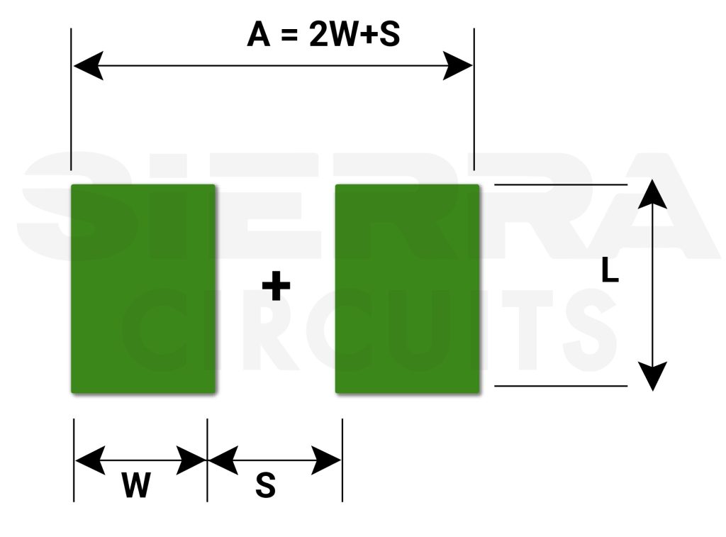
| Component specification | A (2✕component width+spacing between two adjacent components) | W (Component width) | S (Spacing between two components) | L (Component length) |
|---|---|---|---|---|
| 01005 | 24 | 8 | 8 | 8 |
| 0201 | 34 | 12 | 10 | 12 |
| 0402 | 58 | 20 | 12 | 23 |
| 0603 | 95 | 37 | 21 | 37 |
| 0805 | 120 | 55 | 30 | 45 |
| 1206 | 200 | 70 | 70 | 65 |
| 1210 | 200 | 110 | 70 | 65 |
- The image below shows various component mounting styles (A, B, and C).
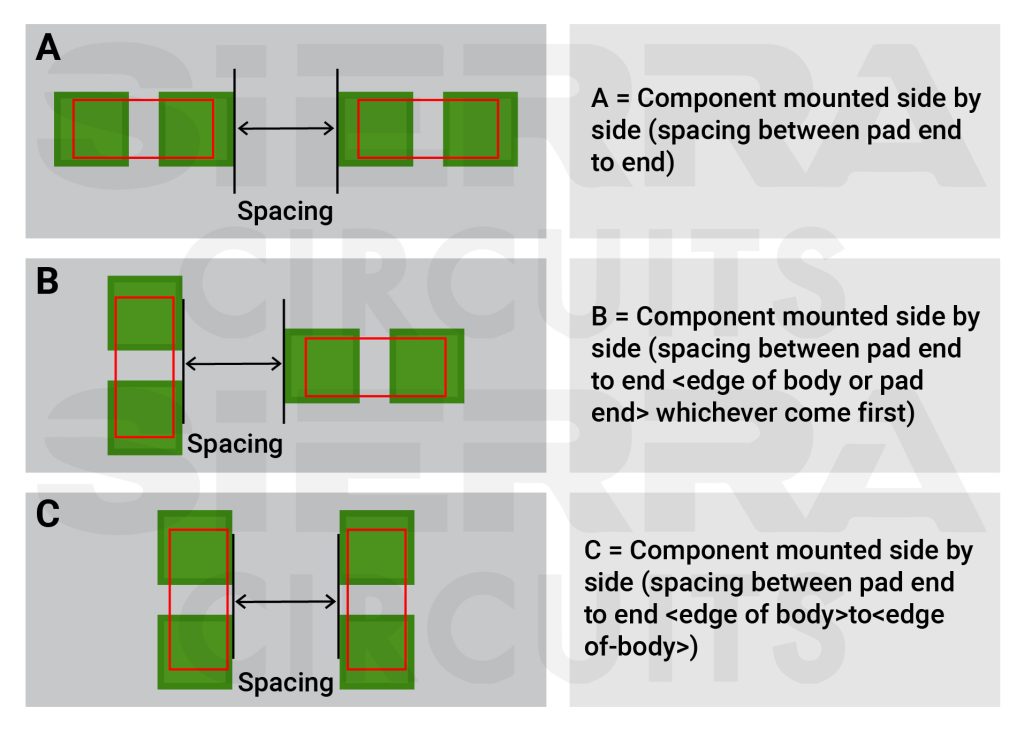
- The following table illustrates the minimum spacing required between two components mounted in 3 different styles (A/B/C):
| Component type | 0201 | 0402 | 0603 | 0805 | 1206 | ||||||||||
|---|---|---|---|---|---|---|---|---|---|---|---|---|---|---|---|
| Mounting style | A | B | C | A | B | C | A | B | C | A | B | C | A | B | C |
| 0201 | 12 | 15 | 10 | ||||||||||||
| 0402 | 12 | 15 | 10 | 12 | 18 | 10 | |||||||||
| 0603 | 12 | 18 | 10 | 15 | 20 | 10 | 15 | 20 | 12 | ||||||
| 0805 | 15 | 20 | 12 | 18 | 20 | 15 | 18 | 25 | 15 | 20 | 30 | 18 | |||
| 1206 | 15 | 20 | 12 | 18 | 25 | 15 | 20 | 25 | 18 | 25 | 30 | 20 | 25 | 30 | 20 |
5.2 Component-to-hole spacing
- Minimum part-to-hole wall spacing: 8 mil
- For manual soldering, part-to-hole wall spacing: 50 to 100 mil
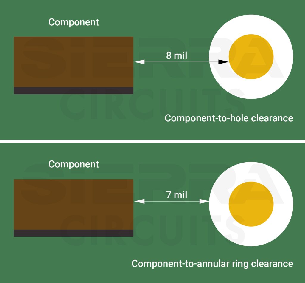
5.3 Component-to-annular ring spacing
- Minimum component-to-annular ring spacing: 7 mil
5.4 Component-to-edge spacing
The table below outlines the distances between the board edge and larger, smaller, and manually soldered components.
| Clearance between the part and board edge | |
|---|---|
| Larger components (BGAs) | 125 mil |
| Smaller components | 25 mil |
| Manually soldered components | 10 mil |
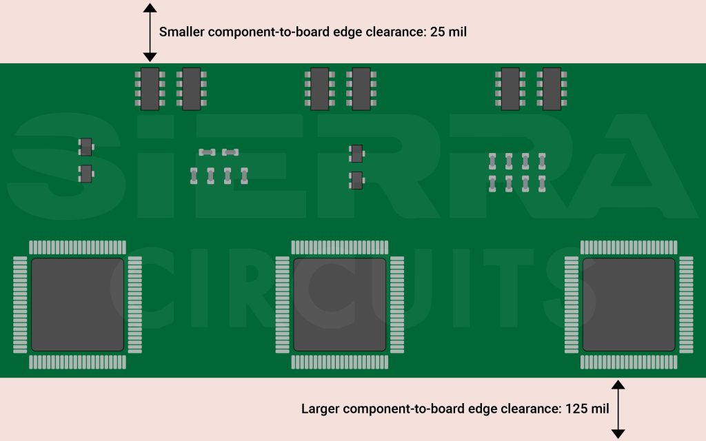
Placing components in close proximity could make the soldering and assembly process more difficult, thereby increasing assembly costs. For strategies to keep the assembly expense down, see how to reduce PCB assembly cost.
6. Include the right solder mask clearances to avoid pad overlapping
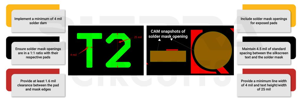
- Implement a minimum of 4 mil solder dam to prevent pad encroachment.
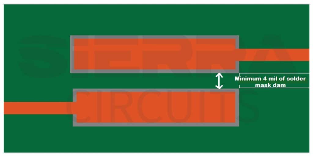
- Verify solder mask openings are in a 1:1 ratio with the respective pad.
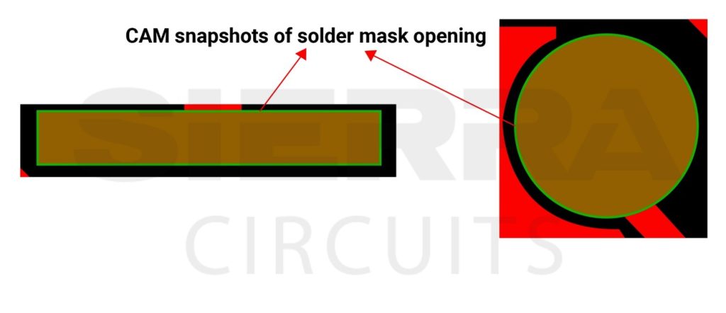
- Provide at least 1.6 mil clearance between the pad and mask edges.

- Design solder mask openings for exposed pads, such as thermal pads and grounding pads.
- Maintain 4.5 mil of standard spacing between the silkscreen text and the solder mask.
7. Ensure silkscreen legibility
- Avoid overlapping reference designators to ensure legibility.
- Provide a minimum line width of 4 mil and text height of 25 mil for better readability.

- Ensure reference designators are clear on the silkscreen layer.
- Always use the standard white color.
- Validate logo and date format requirements.
8. Incorporate test probes near the component legs to ease the testing procedure
- Estimate the minimum distance between a test point and the component by the formula:
L = (0.29 x Height) + 0.7 (in mm)
E.g. For height H= 4 mm, L= (0.29 x 4)+ 0.7 = 1.86 mm
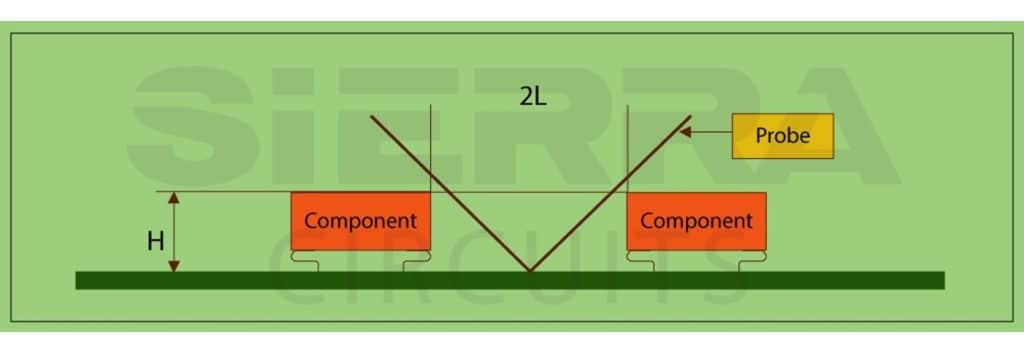
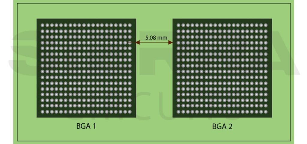
- Avoid placing a test point under a BGA component because it includes tiny solder balls underneath, which can obstruct test point accessibility.
- Moreover, to correctly position the test points, leave at least a 5.08 mm gap between two adjacent BGA components.
- For SMD components, the pad should be longer than the component pin. This enables the testing probe to contact the test point not on the pin but on the pad itself.
- Incorporate test probes near the component legs in order to inspect for any potential open circuit.
For more on DFT, download the Design for Testing Handbook.

Design for Testing Handbook
7 Chapters - 28 Pages - 45 Minute ReadWhat's Inside:
- PCB testing strategies
- Guidelines to design and place a test point for FPT
- Directives to make your board ICT compatible
- Benefits and drawbacks of various testing methods
- Defects that you can identify through board testing
Download Now
9. Provide optimum spacing between the boards during panelization
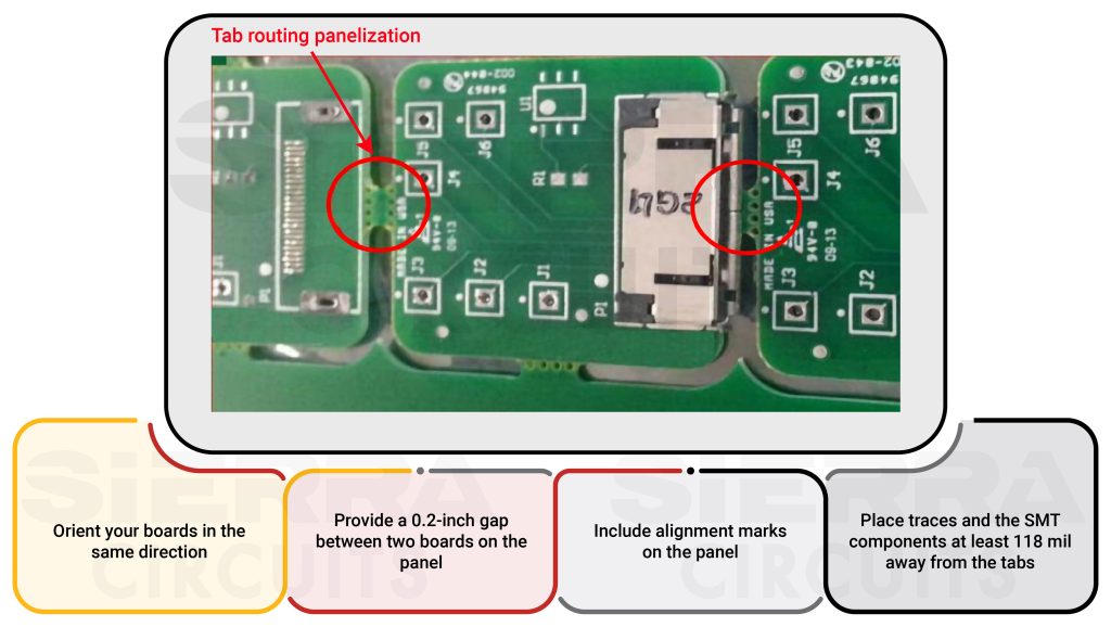
- Orient your boards in the same direction to accommodate the maximum number of boards in an array panelization.
- Provide a 0.2-inch gap between the two boards on the panel to prevent damage during depanelization.
- Include alignment marks or fiducials on the panel.
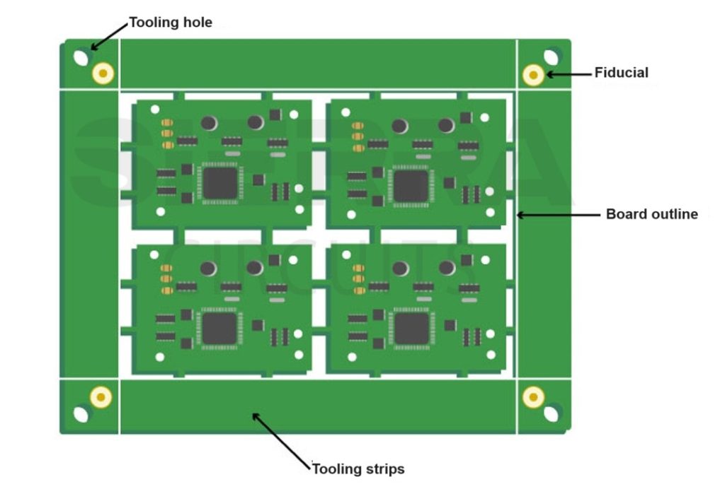
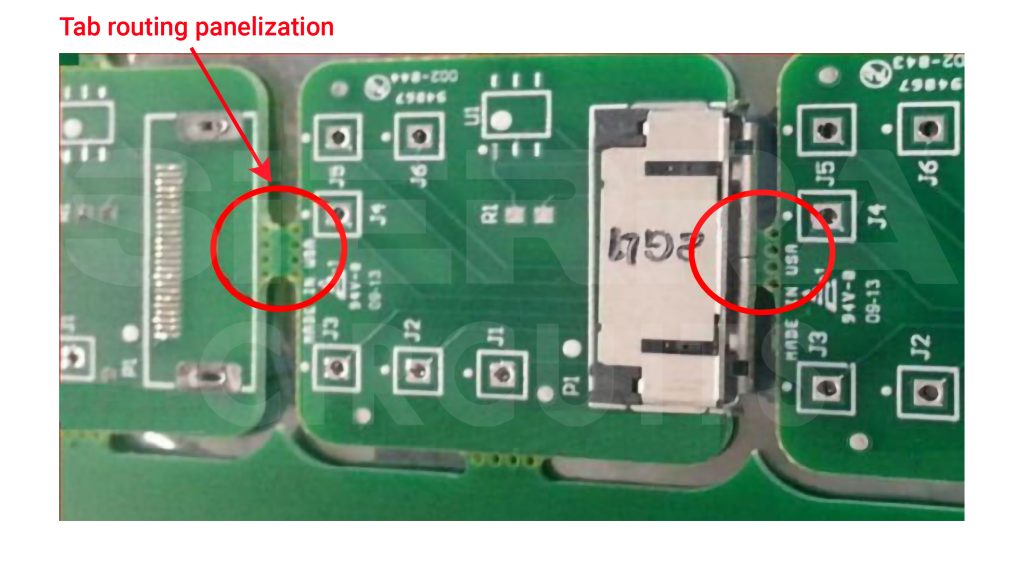
- Ask your CM to avoid V-scoring when there are components hanging over the edges. Clearly mention the requirement of circuit board jump scoring on your fab drawing as a table score.
- Place traces and the surface-mount components at least 118 mil away from the tabs.
- To avoid both mechanical and electrical damage, do not locate perforated tabs adjacent to sensitive components.
Read our interview with Harry Kennedy, Electrical Engineer, at Altair, where he talks about optimizing circuit board designs for testing.
Key takeaways
- Footprints should precisely align with the component’s physical dimensions as specified in the datasheet
- Define pin 1 and polarity markings in the footprint and assembly drawing
- Specify the right component quantity, MPN, and description in your BOM
- Group the components based on their functionalities, current, and voltage levels
- Component-to-annular ring and component-to-hole clearances should be 7 mil and 8 mil, respectively
- Incorporate 1.6 mil of solder mask clearance to avoid short circuits between adjacent pads
- Avoid overlapping silkscreen texts to ensure legibility
- Provide a 0.2-inch gap between individual boards on the panel to avoid damage during the depanelization
PCB design for assembly checklist is pivotal to ensuring error-free circuit board assemblies. This also helps you significantly enhance manufacturability by meticulously addressing factors such as accurate footprint design, clean BOM, strategic component placement, optimal solder mask clearances, and silkscreen checks.
This proactive DFA checklist not only results in faster assembly times and reduced project costs but also leads to increased production yield.
Need assistance in implementing these techniques in your design? Post your queries on our PCB forum, SierraConnect. Our design and assembly experts will resolve them.
About Poulomi Ghosh : Poulomi is a microwave engineer specializing in EMI, EMC, RF, and high-speed electronics. As a senior technical writer at Sierra Circuits, she creates advanced engineering articles and webinars for hardware engineers and PCB designers.








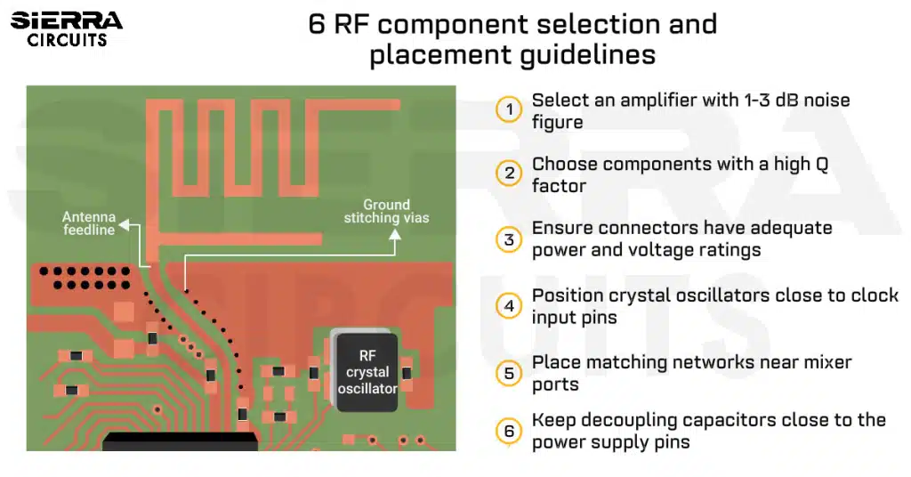
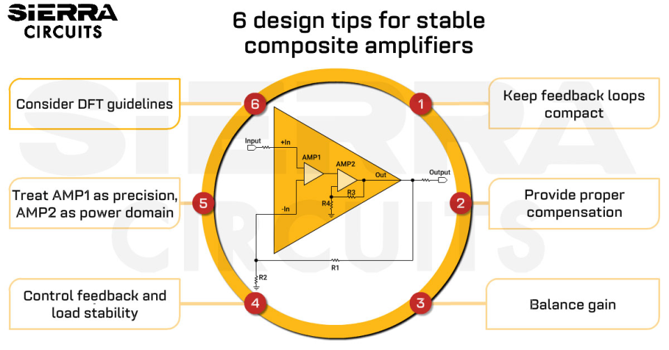


I am designing an HDI board with a 2V operating voltage. Does the recommended 1.6 mil clearance between the solder mask and pads apply here?
What soldering process do you recommend for through-hole components?
For your HDI board with a 2V operating voltage, you can reduce the mask-to-pad clearance to 1.2 mil.
We prefer pin-and-paste soldering for through-hole components. This method eases the soldering process by minimizing the solder volume and facilitating the efficient placement of small components, especially in HDI designs. Additionally, it contributes to temperature control during the soldering process.
Really appreciate this post.
Can also be called PCB Release Checklist. Or PCB 101
Thanks for the good info