


Contents
HDI designs pose complex routing challenges due to their tight spacing between components and traces. Using DRC settings in advanced design tools, opting for smaller packages, implementing thermal management strategies, and early collaboration with manufacturers can help you navigate through these challenges.
Highlights:
- Route adjacent differential signal pairs with a 3W separation to minimize cross-coupling effects.
- Prefer integrated components such as SMDs, BGAs, and chip-on-board to minimize space usage.
- Consider advanced dielectric materials with higher thermal conductivity, like Isola I-Tera MT40, for power and ground planes for improved thermal performance.
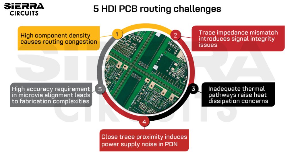
5 HDI PCB routing challenges with solutions
1. High component density causes routing congestion

Placing the components optimally on HDI PCBs to create adequate space for routing can be complex. Here are 4 potential challenges you may face while routing due to dense component layout:
Space constraints: HDI PCBs are characterized by their higher trace and component density. Numerous components must be accommodated within a limited space. This leads to congestion.
Signal integrity issues: Inappropriate component placement can negatively impact the signal integrity of your design. For instance, placing sensitive components closer to heat-generating, at the board’s edge, or providing insufficient clearance between components, can cause EMI, crosstalk, and impedance mismatches. For ultra-HDI PCB design considerations, see designing and fabricating ultra-HDI PCBs.
Thermal difficulties: In HDI layouts, components are placed nearby. This raises concerns about heat concentration and effective thermal dissipation. As a PCB designer, you should not route critical lines such as clock signals, data buses, and ground through the hotspots.
Manufacturing complexities: Poor component placement and routing can result in various manufacturing defects, such as misaligned layers and inaccurate drill holes. This further leads to difficulties in soldering and assembly.
Need assistance in routing your HDI layout with signal integrity? Check out our PCB design support.
13 component placement guidelines for HDI
- Group components that perform the same function. This can be done by grouping components connected to the same signal or with the same electrical characteristics. This alleviates HDI PCB routing challenges, congestion, and minimizes mutual interference.

Grouping circuits with similar VCC and GND to mitigate HDI PCB routing challenges - Maintain sufficient spacing (4 to 8 mil based on the copper thickness) between traces and nearby components.
- Place high-speed components, connectors, and specialized ICs first to create shorter signal paths, minimizing signal attenuation.
- Utilize design rule-checking tools in your PCB design software to catch clearance and spacing constraint violations during the design process.
- Avoid oversized footprints (0805/C-packs), as they can hinder efficient routing. Instead, opt for 0402 or 0603 components. Optimize your PCBA with our comprehensive component placement guidelines.
- Choose integrated components such as SMDs, COB, and BGAs. This reduces space consumption and allows for more efficient layout arrangements.
- Select components with a package that closely matches the calculated trace width to reduce impedance mismatches.
- Place noise-sensitive components, like analog circuits, away from noisy components, such as high-frequency digital circuits, to minimize interference.
- Employ ground planes (copper pours) adjacent to sensitive signal traces to create a shield that helps prevent unwanted interference from affecting the signals. This also shortens the return path.
- Incorporate rounded pads to route traces closer to the pads. The absence of sharp corners allows for shorter, more direct connections, reducing the overall length of signal paths and creating compact circuitry.
- Place high-current components closer to the power plane to minimize the overall loop length. This helps mitigate voltage drops and ensure uniform power distribution throughout the PCB.
- Noisy components such as high-speed processors should be placed on separate ground planes to contain EMI.
- Do not place components or vias between differential pairs. Components and vias create a discontinuity in impedance and could lead to signal integrity problems.
To learn how we resolved the issues while designing a circuit board with microcontroller and antenna signals, see our case study, designing microcontroller and functional PCBs with an antenna.

HDI PCB Design Guide
5 Chapters - 52 Pages - 60 Minute ReadWhat's Inside:
- Planning your stack-up and microvia structure
- Choosing the right materials
- Signal integrity and controlled impedance in HDI
- Manufacturing considerations for higher yields
Download Now
2. Trace impedance mismatch introduces signal integrity issues

The primary cause of signal integrity issues in PCBs is faster signal rise times. Circuit board designs usually encounter fewer problems with signal integrity at low-to-moderate frequencies. The challenges become more significant when operating at higher frequencies.

Some of the common hurdles faced in maintaining the signal integrity in HDI circuit boards during routing are:
Unregulated line impedance: High-speed signals can encounter impedance mismatches at vias and connectors or when trace widths change, leading to signal reflections.

Crosstalk: In densely routed boards, adjacent traces can couple, leading to crosstalk. This interference can distort signals and impact the overall circuit board performance.

Skew and timing issues: High-speed signals traveling across different trace lengths or layers can experience skew due to uneven line impedance, causing timing misalignment. This can lead to synchronization problems in data transmission.
9 methods to tackle signal integrity issues in high-density boards
- Increase spacing between high-speed signal traces to reduce coupling capacitance and minimize crosstalk.
- Route differential pairs with proper separation of minimum 3W between the adjacent pairs to reduce cross-coupling effects. Maintain a 30-mil keep-out zone from other signals, increasing it to 50 mil for clocks or periodic signals to ensure proper isolation.

Maintain 3W spacing between adjacent differential pairs. - The spacing between two traces within a differential pair should not surpass twice the width of the traces. For instance, if a differential trace measures 4 mil in width, the space between them should not exceed 8 mil. Additionally, ensure that the trace width does not surpass twice the dielectric thickness between the intended signal layer and the nearest reference layer.
- Arrange traces that are prone to crosstalk at right angles to each other. This reduces the coupling between them.
- Maintain a minimum distance of 4 times the trace width between adjacent copper in a single serpentine trace to reduce crosstalk. Further, ensure each segment of the bends is 1.5 times the trace width. Many CAD tool DRCs may not verify these distances for traces within the same net.

Distance between adjacent copper in a single serpentine trace to reduce crosstalk - Surround sensitive traces with ground or guard traces that act as barriers, shielding signals from adjacent traces to minimize electromagnetic coupling.

Guard traces for sensitive signals to reduce crosstalk - Implement length-matching techniques to ensure signals arrive at their destinations simultaneously to minimize signal skew.
- Compensate the length near the origin of the trace to ensure the positive and negative signal components are propagated synchronously over the connection.

Length matching in a differential pair - If there are bends that act as the source of length mismatches, implement the compensation very close to the bend.

Adding length compensation in a differential pair - Minimize the use of vias in such critical signal paths to reduce skew.
- Compensate the length near the origin of the trace to ensure the positive and negative signal components are propagated synchronously over the connection.
- Use a solid ground plane beneath and in between high-speed signal layers. This provides a reference plane for signal return paths and minimizes crosstalk. Also, multiple vias can be used for a low-inductance connection to the ground plane.
- Avoid routing traces over a split plane or a void in the reference plane, which can cause degradation of the electrical signal. If unavoidable, use stitching capacitors to provide a return path for high-frequency current and reduce current loop area, minimizing impedance discontinuity caused by split plane traversal.
For more on signal integrity, read 10 HDI PCB design tips to maintain signal integrity.

Signal Integrity eBook
6 Chapters - 53 Pages - 60 Minute ReadWhat's Inside:
- Impedance discontinuities
- Crosstalk
- Reflections, ringing, overshoot and undershoot
- Via stubs
Download Now
3. Inadequate thermal pathways raise heat dissipation concerns

Heat dissipation becomes significant when the components and traces are packed closely. Proper heat management prevents overheating, component degradation, and potential system malfunctions.
Some of the major concerns that you need to consider are:
Limited thermal pathways: Insufficient thermal pathways in HDI layout can lead to localized hotspots, elevated temperatures, and potential thermal-related issues.
Thin dielectric material: Thin dielectric materials have lower thermal conductivity than thicker materials. Most PCB substrates have a thermal conductivity of 0.3 to 0.6 W/M-ºC, which is quite low. This means they are less effective at conducting heat away from the components.
Implications of layer stacking: The arrangement of different layers in a high-density circuit board, especially the power and ground planes, can have a significant impact on how heat is conducted, distributed, and dissipated. Proper layer placement helps spread the heat uniformly, preventing concentration in specific areas. Uneven distribution can lead to localized hotspots, affecting the thermal performance and reliability of the HDI circuitry.
8 ways to improve the thermal performance of HDI PCBs
- Use thermal vias to transfer heat between different layers. These vias act as thermal paths for conducting heat away from hotspots.

Thermal vias placement in the circuit board. - Use cooling fans to improve heat dissipation. These fans increase the airflow and offer active cooling that reduces heat buildup and stops overheating.
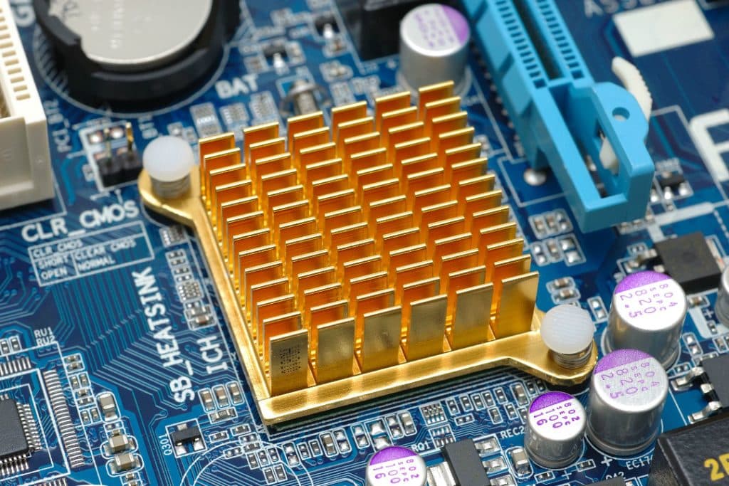
- Attach heat sinks to heat-generating components, such as switching devices, to provide passive cooling. Heat sinks are thermally conductive metal components that efficiently dissipate heat from hot components and spread it over a larger surface area.
Heat sink connection to the circuit board - Avoid clustering components that generate significant heat in close proximity to each other.
Keven Coates, a senior avionics electrical engineer, says, if dealing with a lone heat-generating component, place it at the board’s center for optimal thermal dissipation. Conversely, for multiple heat-generating components, distribute them across the board to ensure uniform heat distribution and prevent localized heating.
For more expert tips on thermal management, see PCB heat dissipation techniques by Keven Coates.
- Minimize the length of traces carrying high-current signals or power. Shorter traces have lower resistance and, therefore, generate less heat. In addition to this, the trace width should be increased to reduce resistance and inductance effectively.
- Select the appropriate copper thickness to minimize signal loss, enhance power efficiency, and effectively manage thermal challenges. High resistance in copper traces and vias can lead to substantial power loss and heat generation. Always adhere to IPC-2141 and IPC-4562 standards to determine the trace width.

Physical dimensions of a PCB trace 
- Use thicker copper for power and ground planes to enhance their thermal conductivity. Thicker copper layers can improve these planes’ ability to distribute and dissipate heat. Advanced dielectric materials such as Isola I-Tera MT40 offer higher thermal conductivity for power and ground planes. This enhances the overall thermal performance of your PCB.
- Utilize thermal simulation tools to analyze the impact of the layer arrangement on heat distribution. Simulations can help identify potential hotspots and guide adjustments to the layer stack-up for improved thermal performance.


For more PCB heat dissipation techniques, see 12 PCB thermal management techniques to reduce PCB heating.
4. Close trace proximity induces power supply noise in the PDN

Power integrity is a subset of signal integrity. A robust PCB design will deliver stable and noise-free power to all components on the board.
Some of the common power integrity factors you need to consider while routing your HDI board are:
Simultaneous switching noise (SSN): The simultaneous switching noise or ground bounce refers to a noticeable shift in the ground potential near a switching IC, typically toward a non-zero value. The simultaneous switching leads to a momentary increase in the ground voltage within the device compared to the system ground. Subsequently, ground bounce can degrade the noise margins, leading to unwanted noise in the system.
PDN impedance: In HDI designs, the power planes are often divided into smaller sections due to increased signal layers. This can increase impedance in the power distribution network, leading to increased voltage drop and noise on the power supply lines.
10 routing techniques to optimize the power distribution network in HDI
- Place decoupling capacitors near the power pins of high-speed components. This minimizes SSN, mitigates voltage fluctuations, and stabilizes power delivery. Learn how to use a decoupling capacitor to implement it in your circuit board design accurately.

Decoupling capacitor on the line trace - Employ multiple decoupling capacitors of varying capacitance values to filter different frequency components of the power supply noise. Smaller capacitors between 0.01 µF to 0.1 µF work well for higher-frequency noise, while larger capacitors between 1 µF to 100 µF handle lower-frequency noise.

Arrangement of decoupling capacitors in PCBs - Maintain a stable reference voltage to minimize ground bounce. Use individual ground vias for each component.
- Utilize ground pours and do not split the power plane to minimize the effect of increased PDN impedance. Plane splits can introduce impedance variations and lead to voltage drop issues.
- Allocate dedicated power and ground planes on inner layers of the HDI PCB stack-up close to signal layers. This allows for efficient power distribution, minimizes loop areas, and reduces impedance.
- Use ground planes between signal and power layers to provide shielding and reduce interference.
- Utilize stitching vias to connect power and ground planes. This helps create short current return paths, reducing impedance.
- Keep signal and power traces isolated to prevent power noise from coupling into signals and reduce the risk of EMI and crosstalk.
- Place a bypass capacitor as close to the component’s supply pin as possible to effectively bypass the voltage spikes and power supply noises. This capacitor acts as local charge storage for switching components like transistors. The additional voltage spikes are stored in this capacitor and not circulated through the circuit. Therefore, all the ground points will have the same potential, and ground bounce will not occur.

Noise elimination using a bypass capacitor - Choose vias with low resistance for power distribution. Blind and buried vias can be particularly useful for reducing via resistance.
To mitigate power supply noise, read 4 common PDN design challenges and how to resolve them.
5. High accuracy requirement in microvia alignment leads to fabrication complexities
HDI designs demand advanced manufacturing techniques, such as sequential lamination, as they must accommodate microvias, fine-pitched traces, and multiple routing layers. This leads to several fabrication complexities that manufacturers must overcome to produce reliable HDI boards with accurate routing.

Here are some potential fabrication issues you must consider during the routing process:
Precision drilling and alignment of microvias: Microvias, due to their miniature size, require extremely precise drilling using lasers. This demands advanced drilling equipment capable of achieving the required accuracy. Also, any misalignment can result in electrical discontinuities, rendering the design non-functional.

Microvia aspect ratio management: Microvias often have a high aspect ratio (0.8:1), creating challenges during plating. Hence, ensuring uniform copper deposition throughout the via’s depth becomes intricate.

Tight trace spacing: In high-density boards, the traces are closely spaced, requiring advanced etching and plating processes to maintain isolation.
Microstrip and stripline routing: HDI PCBs may incorporate microstrip and stripline routing for controlled impedance. Achieving consistent impedance values across the board is challenging.
9 best routing practices to streamline the HDI fabrication process
- Clearly mention the aspect ratio, clearances, and layer-to-layer alignment tolerances in your fab notes. This helps your CM understand your requirements well. Sierra Circuits employs advanced Hitachi drilling machines that can achieve a 1-mil hole placement tolerance, known as drill true position. This precision is accomplished through vision drill systems, enabling you to create designs with annular rings of less than 3 mil for specific layer counts.
- Design the circuit board stack-up in accordance with the IPC-2226 standard to ensure microvia manufacturability. It assures efficient heat dissipation that can prevent thermal stress on the microvia.
- Maintain consistent annular ring dimensions around microvias. This helps prevent misalignment due to variations in drilling accuracy and ensures reliable connections. Further, consider landless via technology incorporating laser drilling techniques to reduce the annular ring, where pads may not be needed at all. Landless vias significantly enhance routing density on HDI boards (2X-4X), especially for bus routing, where the vias can be invisible, matching the trace width (100 microns, 75 microns, or 50 microns).
Happy Holden, HDI PCB design expert, says, “Landless vias are a little-known secret of some of the world’s largest OEMs like IBM, Hewlett-Packard, NEC, and Fujitsu.”

Annular ring layout - Select the appropriate microvia arrangement for your design. Depending on the layer transition and required aspect ratio, you may opt for stacked or staggered vias. Each arrangement has its benefits and considerations.

Stacked and staggered microvias - Avoid exceedingly high aspect ratios of microvias as much as possible because they can make the drilling and plating procedures more difficult and lead to production flaws. The ideal aspect ratios for through-holes and microvias are 10:1 and 0.8:1, respectively.
- Implement staggered arrangements to help improve the effective aspect ratio. This reduces the copper required to fill the via, which is time-consuming and expensive. Stacked vias should be filled and planarized.
- Maintain an adequate spacing of 3W or a minimum of 2W between controlled impedance traces and components (the rule does not apply to differential pairs).
- For stripline construction, use unbroken power/reference planes adjacent to the differential pairs. The adjacent ground planes act as return current paths and reduce EMI issues.
- Work closely with the PCB manufacturer to ensure the design aligns with their fabrication capabilities. These solutions help maintain design integrity while ensuring manufacturability.
To learn how we overcame EMI and routing issues in a medtech PCB, see case study: resolving EMI and PCB routing issues in a medical optical scanner
13 DRC factors to keep in mind before routing an HDI board
PCB design rule checking (DRC) is a critical step in the design process that involves automated software tools checking the design against predefined rules and constraints. DRC is essential for identifying and correcting potential issues before the PCB is fabricated, reducing the risk of errors and costly rework.
- Minimum trace width and spacing: Determine the minimum trace width and spacing your fabrication process allows. HDI designs typically involve narrower traces and smaller spaces, so be aware of these specifications.
- Annular ring size: Check the minimum annular ring requirements for vias and component pads. HDI designs often require tighter annular rings due to smaller via drill sizes and increased component density. As per IPC, a class-2 board requires:
- A minimum annular ring of 2 mil for laser-drilled vias
- A minimum annular ring of 4 mil for mechanically drilled vias
- A minimum annular ring of 10 mil for through-hole components
- 8 mil drill to copper on the inner layer
- Drill size and aspect ratio: Understand the minimum via drill size and aspect ratio (hole diameter to board thickness). Ensure your design’s vias fall within acceptable limits for the chosen PCB fabrication process.
- Copper-to-edge clearance: Verify the required copper-to-edge clearance. Make sure it complies with the manufacturing capabilities of your chosen PCB manufacturer.
- Solder mask openings: Confirm that solder mask openings are correctly defined. These openings should adequately cover exposed copper areas, preventing solder bridges during assembly.
- Copper feature sizes: Know the minimum and maximum copper feature sizes your CM allows. This includes pad sizes, trace widths, and via sizes.
- Stacked vias and via-in-pads: If your design includes stacked vias or vias-in-pads, verify that these meet the manufacturer’s specifications, including drill registration and minimum feature sizes.
- Thermal relief: Define thermal relief connections for components, if any. Ensure that thermal relief patterns align with manufacturing capabilities.
- Trace-to-trace spacing: Attention to the minimum spacing between traces, especially in high-speed designs. Proper spacing helps prevent crosstalk and signal integrity issues.
- Keep-out zones: Clearly define keep-out zones for sensitive components (such as connectors) and RF zones or areas where no traces or vias should be placed.
- Layer stack-up: Verify that the layer stack-up is accurately defined and adheres to manufacturer guidelines. Additionally, consider factors like core materials, prepreg thicknesses, and the placement of signal and ground planes.
- Silkscreen and reference designators: Ensure that silkscreen markings and reference designators are appropriately placed and legible. These markings provide critical information for assembly and testing.
- Manufacturability guidelines: Collaborate closely with your PCB manufacturer to understand their specific DRC guidelines and capabilities. This collaboration is essential to ensure that your design aligns with manufacturing requirements.
By considering these DRC factors and working closely with your manufacturing partner, you can increase the chances of a successful HDI PCB design that meets design and manufacturing standards.
6 things to consider when choosing an EDA tool for HDI routing
1. Layer stack-up management: Look for an EDA tool with robust layer stack-up management capabilities. This feature is essential for accurately configuring your PCB layers, including signal, power, and ground planes.
2. Routing capabilities: The EDA tool should have advanced routing capabilities such as interactive routing and length matching for high-speed signals, differential pairs, and controlled impedance routing.
3. Auto-placement: Design tools with automated placement can help optimize the placement of components, vias, and routing elements on the layout. This can help minimize signal interference, ensure optimal use of space, and adhere to design constraints. Automated placement is especially beneficial in HDI designs, where precise component positioning is crucial for achieving a compact and efficient routing layout.
4. Custom libraries: The tool should allow you to create and maintain custom component libraries tailored to your specific project needs. This ensures consistency and streamlines the design process, saving time on repeated tasks.
5. Design rule checks (DRC): The EDA tool should allow you to regularly run DRCs to catch potential errors early in the design process. Configure DRC settings based on project requirements to ensure manufacturing and performance standards compliance.
6. Auto grouping: Auto grouping for repetitive functions is an essential feature that allows you to replicate repeated or identical elements within a design efficiently, saving time and effort. This feature is particularly valuable when dealing with designs that involve repeated components, such as arrays of similar structures, buses, or modules.
Key takeaways:
- Choose smaller packages and integrated components (SMDs, COB, BGA) to reduce space occupation.
- Maintain sufficient spacing (4 to 8 mil) between traces and nearby components to prevent unintentional connections and shorts.
- To reduce skew, use serpentine traces at the origin of length mismatching and minimize the use of vias in signal paths.
- Arrange traces prone to crosstalk at right angles to each other to reduce coupling.
- Use higher copper weight for power and ground planes to enhance their thermal conductivity.
- Maximize the size of the ground and power planes to increase the heat dissipation.
- Place decoupling capacitors near high-speed component power pins to minimize simultaneous switching noise and stabilize power delivery.
- To facilitate drilling and plating procedures, avoid exceedingly high aspect ratios (ideal 10:1 for through-holes, 0.8:1 for microvias).
- Maintain spacing of 3W or a minimum of 2W between controlled impedance traces, other traces, and components.
- Assign specific layers for critically controlled impedance traces with unbroken ground planes.
- Use design rule-checking tools to identify design violations during the design process.
High-density circuit boards offer significant benefits for advanced electronic systems but present challenges in fabrication, signal integrity, and thermal management. However, you can overcome these challenges with careful planning, utilizing advanced design tools, collaboration with manufacturers, and adherence to best practices.
Need assistance in designing your HDI PCBs? Post your queries on SierraConnect. Our experts will be happy to resolve them.

About Pooja Mitra : Pooja Mitra is an electronics and communication engineer. With an experience of over three years in the PCB industry, she creates industry-focused articles that help electrical and PCB layout engineers.


Given the potential for increased heat generation in 5G devices, how do you address thermal management in HDI designs, and what impact does it have on routing configurations?
What are the key considerations when routing microstrip and stripline traces in HDI boards for RF applications?
To address increased heat generation in 5G devices, especially in HDI designs with smaller BGA sizes and higher processing power, large Cu surfaces and air gaps are utilized to efficiently transfer and dissipate heat. A few strategies, such as using low-height components surrounding the BGA, keeping a few solder masks open at the bottom of the BGA’s, utilizing ground planes as heat sinks, implementing thermal vias for QFN ICs, transferring heat to metal chassis, and using untented vias can aid in effective heat dissipation. Further, increasing the number of vias on the power plane helps mitigate hotspots. These strategies can influence the spatial arrangement of components and how they are connected. Additionally, thermal considerations often lead to adjustments in trace widths and spacing to disperse heat effectively while maintaining optimal signal integrity.
Striplines are generally avoided for SMA connections in RF applications, and microstrip configurations are preferred. It has to follow a co-planar structure where vias are added at a regular interval on the boundary of the two Cu ground pours with a spacing less than λ/10, where λ is the wavelength of the highest frequency content in the signal. Typically, we maintain a spacing of 20-30 mils for vias to ensure optimized routing space in internal layers. In cases of through-hole SMA connectors, it’s crucial to avoid unintended stubs. If stubs are unavoidable, their length must be carefully managed based on the signal frequency requirements. The length of the trace should be as short as possible. Additionally, incorporating reference planes on adjacent layers is essential for optimal performance.