


Contents

On-demand webinar
How Good is My Shield? An Introduction to Transfer Impedance and Shielding Effectiveness
by Karen Burnham
Designing PCBs for 5G and IoT applications demands high performance, low power consumption, and reliable connectivity. 5G surpasses 4G with significantly higher transmission rates, expanded data capacity, lower latency, and the utilization of millimeter-wave frequencies.
This brings forth several crucial considerations that you should take into account when designing PCBs for telecommunication and IoT devices.
In this article, you’ll learn the ways to overcome the challenges in designing a 5G circuit board.
Highlights:
- RT/duroid 5880 is considered the best material option for RF PCBs.
- Activate sleep mode during idle periods to power down components, minimizing energy consumption.
- Secure FCC Certification, which is essential for introducing IoT products to the market.
5 challenges to tackle when designing a 5G PCB
5G wireless networks operate within the extremely high frequency (EHF) band, specifically utilizing millimeter-wave frequencies. These frequencies include the sub 6 GHz, 20-40 GHz (low mm-Wave), and 57-95 GHz (high mm-Wave) bands. This allows for faster data transmission and lower latency.
Hence, circuit boards designed for wireless and networking devices come with the dual challenge of supporting higher digital data rates and frequencies. Further, this creates a significant issue for mixed-signal design, which integrates both analog and digital circuitry on the same board.
The layout design considerations for telecom PCBs vary based on whether they are intended for exclusive 5G applications or 5G-enabled IoT devices.
1. High-frequency signal attenuation due to environmental obstacles
Millimeter waves, a characteristic of the EHF band, primarily propagate in a line-of-sight manner. They undergo notable signal attenuation caused by obstacles along the transmission path, including buildings, foliage, or unfavorable weather conditions such as rain or humidity.
Therefore, more base stations are needed for the 5G network to ensure reliable coverage and signal strength due to these wave characteristics.
The use of phased array antennas can address the requirement to support multiple frequencies.
It also supports beamforming, an advanced technique that enables the concentration of the signal in a specific direction, enhancing data transfer.

Hence, the implementation of advanced technology is critical in both mobile devices and base stations. Utilizing PCBs designed to integrate multiple antenna array units (AAU) using massive MIMO (multiple input, multiple output) technology enhances data transfer efficiency and reduces latency.

2. Bandwidth per channel concerns
In the 5G technology, the channel bandwidth is set at 100 MHz for frequencies below 6 GHz and at 400 MHz above 6 GHz. You will find several modems in the market along with RF components that can support this range of channel bandwidth. However, PCB material plays a crucial role in the design process.
Integrating the RF front end, consisting of power amplifiers, low-noise amplifiers, filters, and antenna interfaces, directly onto the board raises demand for materials that showcase minimal dielectric transmission loss and exceptionally high thermal conductivity.
Further, when dealing with frequencies above 6 gigahertz in your circuit board design, it’s crucial to choose materials that specifically suit the characteristics of the millimeter wave frequency band and can efficiently transmit signals at these high frequencies.
To learn how to design a high-speed circuit board, download the High-Speed PCB Design Guide.

High-Speed PCB Design Guide
8 Chapters - 115 Pages - 150 Minute ReadWhat's Inside:
- Explanations of signal integrity issues
- Understanding transmission lines and controlled impedance
- Selection process of high-speed PCB materials
- High-speed layout guidelines
Download Now
3. Designing 5G-enabled IoT circuit boards with low-power requirements
Emerging IoT devices are getting more powerful, with greater computing power, better wireless communication protocols, memory, and faster processing. All these features are crammed into smaller form factors.
The goal is to ensure these devices consume less power, include multiple sensors, lower interference, and minimize power fluctuations in upcoming IoT designs.
When you start working on an IoT circuit board design, you may often begin by choosing the processing unit (e.g., microcontroller or processor) and the amount of memory (RAM and flash) based on the computational needs of the embedded software. This helps determine the power requirements for the device during operation.
Higher processing power and memory often lead to increased power consumption, potentially limiting the device’s mobility or requiring a larger battery, making it bulkier and less portable.
Instead, you should start your design focusing on the power source, directly impacting the product’s usability and practicality. Choosing between a battery-powered device and one requiring a wall outlet can significantly influence the design.
If the device is battery-powered, the design process needs to address questions such as how long the device should operate before requiring a recharge. Hence, this decision should not be an afterthought but rather a starting point in the design process.
4. Embedding wireless modules adds complexity
5G-enabled IoT devices often need to communicate wirelessly for data exchange, which requires integrating radio frequency components.
RF signals have specific requirements and characteristics that demand careful consideration in the design phase. This includes factors such as signal integrity and impedance matching, and it considers RF PCB design factors.
One of the primary concerns is preventing EMI and transmission losses, which can impact the efficiency and range of wireless communication.
Therefore, it is crucial to conduct quality control tests to identify and rectify potential issues early in 5G PCB manufacturing. This helps ensure that the final products meet performance expectations and comply with regulatory standards.
5. Diverse sensors and modules integration in a compact board
IoT devices often incorporate a variety of sensors and communication modules. These can include temperature sensors, accelerometers, and GPS modules. Integrating these components within a limited space requires careful planning.
To learn how to tackle microwave board design roadblocks, see microwave PCB design challenges and ways to overcome them.
5G PCB layout design considerations
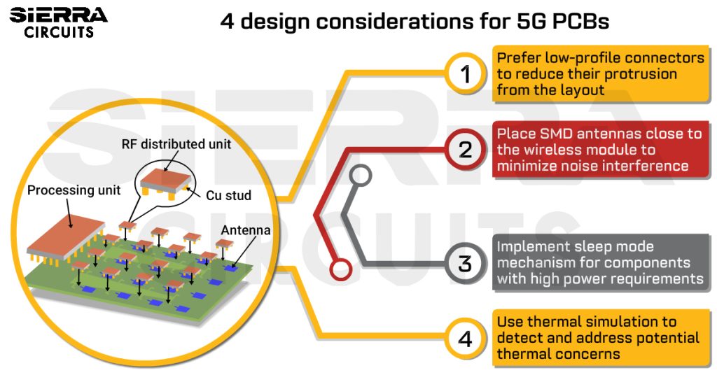
1. Size and form factor constraints
IoT applications often demand boards with a compact form factor to facilitate integration into various devices, ranging from sensors to wearables. The same applies to 5G-enabled devices. As board size decreases, the available board real estate becomes more precious.
IoT devices often incorporate multiple boards for diverse functionalities. The challenge lies not only in the reduced size but also in the need to pack multiple circuit boards into a confined space.
The cavities in which printed boards are housed may have unique shapes or be very thin. Reduced PCB clearance within these cavities becomes a critical consideration in the design process.
One of the critical components contributing to this miniaturization effort is the connectors used on these boards. Smaller connectors allow for more components to be accommodated within the reduced space, enhancing the overall utility of the PCB.
Importance of connector size and protrusion in 5G PCB assembly
Smaller connectors play a pivotal role in addressing the challenges posed by reduced circuit board size and increased board density. The smaller the connectors, the more components can be accommodated, maximizing the utility of the available space. Fine-pitch connectors are commonly used in 5G and IoT PCB designs.
As printed circuit boards get smaller and are packed more densely, the protrusion of connectors from the board becomes a critical consideration. Low-profile connectors emerge as a preferred solution, reducing the height of connectors above the PCB surface and minimizing their protrusion from the board.
8 design tips for a compact 5G and IoT circuit board
- Opt for miniature, high-performance components such as TI CC2650 IC to maximize functionality in a limited space and achieve the delicate balance between size and functionality.
- Implement flexible PCBs for IoT applications where space optimization and adaptability are crucial. Their bendable nature allows for unique form factors and can simplify integration into devices with unconventional shapes.
- Choose system-on-chip (SoC) integration to consolidate functions and reduce the overall footprint of the PCB. This helps optimize space and power usage.
- Adopt a modular design approach to facilitate scalability and adaptability for different size requirements. Design modules that can be easily replaced or upgraded, allowing for future expansion within size constraints.
- Employ efficient thermal management solutions, such as heat sinks and thermal vias, to dissipate heat in compact designs. Also, conduct thorough thermal simulations to identify and address potential hotspots.
- Utilize simulation tools extensively to validate designs before physical implementation. Conduct simulations for signal integrity, thermal performance, power integrity, and electromagnetic interference to identify and rectify issues early.
- Use dogbone and via-in-pad fanout techniques to route high-density BGAs between different layers in your circuit board stack-up.

Dogbone fanout in BGA - Implement controlled impedance routing for high-frequency signals to minimize reflections and distortions.
To learn how to tackle RF via design roadblocks, see 4 RF PCB via design challenges with layout solutions.
2. RF requirements and antenna integration in 5G boards
Designing 5G and IoT products demands meticulous attention to radio frequency design practices. RF plays a critical role in the seamless communication of these interconnected devices. Understanding and managing constraints such as limited space, power consumption, and interference susceptibility early in the design phase sets the foundation for a robust and efficient IoT device.
For more on antenna design, read antenna integration and RF design guidelines for 5G PCBs.
Dielectric material selection for 5th generation RF design
Circuit board material selection is vital in designing a well-optimized PCB for RF integration. Commonly used circuit board materials like FR-4 are cost-effective but not ideal for high-frequency RF applications. This is mainly due to the non-uniformity of the dielectric constant and a less favorable tangent angle. These inconsistencies can result in signal distortion, loss, and compromised performance in high-frequency settings.
5 factors to consider in RF PCB material selection are:
- Moisture resistance: Choose materials with low absorbency (0.02 to 0.08 percent) if your device operates outdoors.
- Dielectric constant– Prioritize materials with a low dielectric constant (less than 4) for RF circuit boards. A low dielectric constant is crucial, especially for high-power circuits, as it measures the material’s ability to store electrical energy.
- Component suitability– Choose capacitors and resistors with characteristics that support stable performance at high frequencies and under varying temperature conditions to meet the specific requirements of RF PCBs. The higher frequency of RF PCBs makes components more susceptible to temperature fluctuations, demanding adherence to sufficient spacing.
- Coefficient of thermal expansion (CTE)– Consider materials with low CTE (within 70 ppm) to withstand high temperatures. Lower CTE allows materials to endure elevated operating temperatures, a critical requirement for RF circuit boards.
- Copper characteristics– Pay attention to the thickness of copper in RF PCBs, as it influences current-carrying capacity and impedance calculations. Use rolled copper that has a very smooth surface with minimal roughness. A rough copper surface exhibits more conductor loss at high frequencies due to reduced skin depth, resulting in propagation delay and insertion loss.

Effect of copper foil surface roughness on high-frequency signals
For more radio-frequency material selection tips, see how to pick RF PCB materials: 6 important factors to consider.
FEP and PTFE, with outstanding electrical properties, low dielectric constant, and heat resistance (over 200°C), are suitable for RF boards. Ceramics, favored for compact designs and thermal stability, are ideal for high-frequency precision. Hydrocarbons and various types of glass fibers strike a balance between electrical performance and mechanical strength, ensuring reliability in RF circuits.
PTFE with fiberglass can be considered the best material option for RF PCB applications if cost is not a constraint. However, if you are looking to lower the cost of the end product, opt for PTFE with ceramic coating, requiring a less complex fabrication process.
When choosing microwave PCB materials, consider Rogers laminates, particularly the RO3000™ and RO4000 series, as they offer reliable performance at high frequencies.
Rogers materials such as RT/duroid 5880, though pricier, cut power losses by 50%, ensuring high performance beyond 20GHz with a stable low dielectric constant. In multi-layered RF PCBs, a cost-effective strategy involves using Rogers laminates for outer layers and more economical epoxy glass laminates for inner layers, meeting electrical and thermal requirements.
At Sierra Circuits, we have extensive experience manufacturing high-frequency circuit boards with PTFE materials. Check out RF and microwave PCB manufacturing services to learn more.
12 strategies for enhanced antenna connectivity in RF boards
- Avoid relying solely on brute-force filtering (a noise filtering method), as it might not provide reliable isolation in RF boards. Implement smart floorplanning methods to arrange circuit blocks strategically on the board, reducing electromagnetic interference and improving the overall design.
- Place antennas within the device’s housing to avoid the impact of external environmental elements.
- Strike a delicate balance between form and function, ensuring that the PCB is compact enough to fit within the device’s constraints while providing ample space for RF components to operate optimally.
- Route high-speed RF signals on external layers over a solid ground plane to avoid impedance discontinuity.

Route critical RF signals on the top layer - Position a surface mount design antenna near the wireless module to shorten the connecting trace length and reduce noise.
- Implement a well-designed large ground plane beneath the antenna, expanding from the feed point in all directions. A solid ground plane enhances antenna efficiency and minimizes the impact of environmental factors on signal quality.
- Explore different locations for antenna placements during the design phase. This helps you test various positions and identify the optimal location for the antenna.
- Plan the layout to include ample distance between multiple antennas, ensuring they are pointed away from each other. This guarantees effective isolation and prevents interference.
- Prioritize meticulous cable routing for flexible printed circuit antennas, considering the device’s form and function. The flexible nature of FPC antennas often means that their cables need to bend and flex along with the antenna. Cables that are flexed or bent repeatedly without proper routing can experience wear and tear, leading to a shortened lifespan of the antenna system.
- Post-design, conduct antenna impedance matching procedures to align the antenna with the RF module to maintain 50Ω impedance.
- Implement the mSAP (semi-additive fabrication process) technique to avoid signal degradation and impedance discontinuity. Unlike the standard subtractive process, mSAP creates precise traces, eliminating the trapezoidal cross-section that hampers trace impedance and poses limitations in 5G applications.

Difference between subtractive process and mSAP - Ensure that the 5G design adheres to compliance requirements of FCC part 15c standard for telecommunication circuit boards.
To know the basics for designing RF and microwave PCBs, download the RF & Microwave Design Guide
RF & Microwave Design Guide
8 Chapters - 44 Pages - 60 Minute ReadWhat's Inside:
- Basics of RF and microwave board design
- Choosing RF materials
- Trace, grounding, via, and stack-up design
- Component selection and placement
- Testing and isolation requirements to avoid interference
Download Now
3. Low power consumption requirements for 5G-enabled IoT PCBs
Optimizing power requirements in your 5G and IoT PCB designs is not just about choosing components with lower power consumption. There are several other considerations that you need to take into account.
10 methods to improve power efficiency in internet-of-things circuit board design
- Select active devices, including MCUs, SoCs/SoMs, FPGAs, and other data-processing ICs, that offer essential processing capabilities with low power consumption.
- Implement a sleep mode mechanism for components with high power consumption during idle periods. In sleep mode, the component effectively shuts down, significantly reducing the power requirement until it wakes up again.
- Explore energy-harvesting solutions, such as solar, kinetic energy, or piezoelectric. Energy harvesting provides a sustainable power source for IoT devices, reducing dependence on traditional batteries.
- Select passive components (resistors and capacitors) and active components (transistors) with minimal leakage currents to avoid unnecessary power loss. These components minimize wasted bias currents.
- Pay attention to cleanliness to improve the overall energy efficiency.
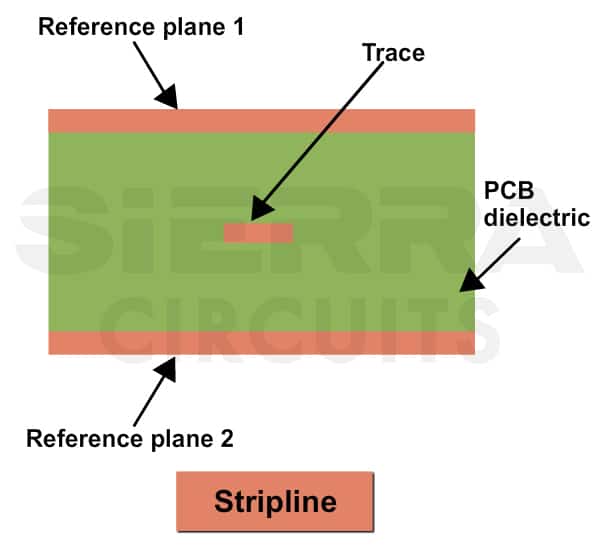
- Design the stack-up to accommodate stripline routing. Consequently, position power and ground planes on adjacent layers. This will enable significant decoupling, reducing the necessity for numerous decoupling capacitors to guarantee power integrity on your board.
Stripline transmission line structure - Opt for sensors and devices with low power consumption, such as Bosch BMA400 accelerometer, Si7021 sensor, and nRF24L01+ wireless module, to ensure that the IoT device operates efficiently while consuming minimal power. This is particularly crucial in scenarios where energy conservation is a priority, such as battery-powered IoT devices.
- Minimize the number of internal peripherals and disable unused ones. Many microcontrollers and SoCs come with various built-in peripherals to accommodate diverse applications. However, not all of these peripherals may be necessary for a specific IoT device. Deactivating the unused peripherals minimizes power consumption as only necessary components draw power.
- Select an MCU that provides different speeds and types of timers and clocks. This flexibility offers multiple ways to adjust the battery drain based on specific operational needs. By dynamically adapting the clock speed and timer settings, the device can optimize its power consumption, conserving energy during periods of lower activity.
- Design the PCB with wide power supply traces to reduce resistance and, consequently, heating losses. This design choice contributes to improved energy efficiency by minimizing the power dissipated as heat, resulting in a more effective use of the supplied power.


4. Thermal management in 5G circuit boards
Massive MIMO makes 5G a possibility, using full-dimensional adaptive beamforming. It is essential to use multiple antennas, each equipped with a transceiver. Further, an RF unit also uses several other blocks like ADCs, DACs, PA, LNA, mixers, and filters, which increases the level of complexity, making it a power-hungry system that makes heat management a critical consideration.
11 best design considerations to dissipate heat effectively in 5G wireless PCB designs
- Identify components on the board with high power requirements that generate the most heat, such as RF transceivers and power amplifiers. These components account for about 75% of the total heat generation. Place such components in areas of the board where heat dissipation can be more effective (board edges).
- Prefer metal core substrates with high thermal conductivity, such as copper, as the base laminate material. This choice enhances the PCB’s ability to dissipate heat efficiently. The metal core serves as a heat sink.
- Use thermal vias in your layout to transfer heat away from the components on the top layer. It provides a pathway for heat to move from the surface components down to the inner layers of the PCB.

Thermal vias to transfer heat from the components on your board - Place heat sinks strategically over high-power components to draw heat away from the components. 5G PCBs often incorporate machined aluminum heat sinks. A thermal interface material, such as thermal grease, insulators with conductive particles mixed into the elastomer, Panasonic’s diamond films, and heat control products offered by Bergquist, can be used between the heatsink and the components to ensure efficient thermal contact. This improves the heat transfer from the components to the heat sink.
- Include cooling fans or ventilation channels within the device’s enclosure to enhance cooling. This active cooling mechanism facilitates hot air exchange with cooler air and maintains optimal operating temperatures for components.
- Incorporate phase change substrate materials. These materials undergo a phase change (e.g., from solid to liquid) as they absorb heat, effectively acting as a thermal buffer. During operation, these materials absorb heat from the components, helping to regulate temperature fluctuations and prevent rapid temperature increases.
- Choose a thinner substrate that will increase the heat flow. Also, select a wider conductor to increase the heat flow path.

Heat dissipation from hotspot to heat sink - Use vapor chambers, which are hollow chambers within the PCB that contain a working fluid. This fluid evaporates at hotspots and condenses in cooler regions. The vaporization and condensation processes within the vapor chamber efficiently transfer heat away from critical areas.
- Use solid power and ground planes to meet the thermal requirements of the design. They act as a heat sink to absorb and dissipate heat away from the components.
- Use thermal simulation software to predict the thermal performance of your PCB design before production. This allows you to detect and address any potential thermal concerns and make necessary adjustments to the design.

PCB thermal simulation in Allegro - Know the anticipated operating temperature range during the design phase since PCBs are influenced by the ambient temperature of their operational surroundings.
Testing, compliance, and certifications for 5G boards
Securing Federal Communications Commission (FCC) certification is essential to introducing IoT products to the market. Further, you must procure UL certification to ensure adherence to safety and performance standards, considering environmental factors like RoHS compliance.
EMC compliance testing and FCC certification for circuit board modules
Designing a 5G or IoT device requires a range of testing to ensure the EM emissions it generates remain within the boundaries defined by FCC rules and regulations. There is a documentation process to certify and register your digital device officially.
You need to obtain complete certification for receiver designs. However, the usage of pre-certified transmitter modules can simplify the process. These modules have already undergone the most rigorous phase of the FCC certification procedure. While you are still required to have your complete system tested for unintentional emissions, the majority of the testing has already been completed.
Key takeaways:
- Phased array antennas and beamforming address attenuation and require advanced PCB design.
- 5G network demands a channel bandwidth of 100 MHz below 6 GHz and 400 MHz above 6 GHz.
- Utilize flexible PCBs and low-profile connectors for space optimization.
- Maintain wide power supply traces, implement efficient sensors, and minimize internal peripherals for improved energy efficiency.
- Plan antenna placement early in the design process for optimal RF performance.
- Place the antennas far away from each other, with each antenna pointing away from the other.
- Manage heat through strategic component placement, the use of thermal vias, heatsinks, cooling fans, substrate selection, and thermal simulation.
- Obtain UL certification to ensure adherence to safety and performance standards, including RoHS compliance.
In 5G and IoT PCB design, designers must leverage advanced technologies such as phased array antennas and beamforming to overcome challenges like signal attenuation, bandwidth issues, diverse sensor integration, and size constraints. Additionally, adherence to industry standards and compliance with regulatory requirements is also key for a successful design.
Need assistance in designing your 5G circuit boards? Post your queries on our PCB forum, SierraConnect. Our design and manufacturing experts will resolve them.

About Pooja Mitra : Pooja Mitra is an electronics and communication engineer. With an experience of over three years in the PCB industry, she creates industry-focused articles that help electrical and PCB layout engineers.


How does the choice of antenna type (e.g., patch, monopole, dipole) impact the performance and efficiency of a 5G PCB design?
How do you address security and reliability concerns in 5G PCB designs, particularly in critical applications such as military and healthcare systems?
Different antenna types have unique radiation patterns, beamwidths, frequency bands, sizes, and gains. The selection of the appropriate antenna depends on board constraints and antenna transmission efficiency. Some antennas offer narrow beamwidth and directivity, while others provide higher gain. All the above-mentioned factors must be carefully considered when choosing the required antenna.
For military and healthcare applications, implement the following security and reliability measures: