


Contents

On-demand webinar
How Good is My Shield? An Introduction to Transfer Impedance and Shielding Effectiveness
by Karen Burnham
AI-assisted circuit board design is reshaping the schematic and layout creation process by recommending optimal part placement and routing topologies. It predicts signal integrity, power integrity, and manufacturability risks in real-time without waiting for the traditional DRC flags or simulation.
At the same time, circuit boards built for AI-driven systems call for 16+ layer, high-density, high-speed boards built with advanced materials to support massive parallel computation.
This article covers two aspects: how artificial intelligence is transforming PCB design workflow and the PCB technologies required to power the next-gen AI hardware.
Highlights:
- Artificial intelligence–driven solvers offer in-design signal, thermal, and power integrity analyses, reducing prototype respins.
- AI systems require advanced PCBs with 16–28 layers, ultra-dense routing, and strict impedance control.
- Low-loss, high-speed materials like Megtron 6/7 and Tachyon 100G are essential for multi-GHz operation.
- High-power applications require robust PDN design, thick copper planes, and high-current VRM arrays.
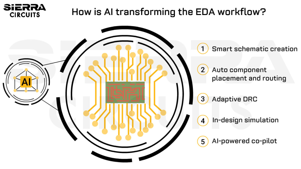
How’s AI changing the PCB design (EDA) workflow?
Artificial intelligence is empowering PCB design tools by automating component placement, routing, and rule checks. It predicts potential design issues early. This enables you to work faster, reduce iterations, and achieve higher-quality layouts with significantly less manual effort.
Let’s break down the AI circuit board design, workflow:
1. Smart schematic creation and component selection
Creating a schematic is a manual process. As a PCB designer, you must interpret functional requirements, choose components, understand constraints, and map everything into a coherent design.
Artificial intelligence is changing this foundational step by automating schematic creation, guiding component selection, and reducing errors early in the design cycle. Let’s look at each of these aspects in detail.
Generate schematics by providing instructions
Modern AI-driven EDA tools allow you to describe functionality in plain English, like “Create a buck converter with a 5V output and 3A load,” and the system generates a schematic draft. This may not be perfect, but it saves hours of manual circuit building.
For instance, using Flux AI, you can create a schematic by providing text-based commands defining the project.

Procure components to ensure supply-chain resilience
Part availability directly impacts design schedules and time-to-market of your application. AI bridges the gap between designers and the procurement team by integrating supply-chain intelligence into the EDA workflow.
AI-powered design platforms are trained on massive component databases. They can:
- Suggest components based on electrical constraints, lifecycle status, and cost
- Flag parts approaching end-of-life
- Recommend pin-compatible alternatives
- Predict supply chain risks for selected components
These suggestions become valuable during shortages or fast product development cycles. AI platforms help you generate accurate bills of materials with reliable alternative part suggestions.
Tools such as Flux AI and Circuitly assist you in making the right component choices by recommending alternatives, analyzing datasheets, and reducing dependency on hard-to-source parts.
Reduce schematic errors
AI can analyze historical design patterns to catch common errors, such as:
- Incorrect power pin connections
- Missing decoupling capacitors
- Improper reference designators
- Configuration pin oversights
These pre-layout corrections reduce DRC issues, speed up routing, and improve final product reliability. In short, the schematic creation phase becomes faster, more accurate, and more data-driven, helping you move to the layout phase with significantly fewer iterations.
2. Auto component placement and routing
PCB layout is among the most time-consuming steps in the design cycle. Standard auto-routers and auto-placement tools have existed for decades, but they often produce suboptimal or inconsistent results, especially in high-speed designs. AI-assisted circuit board design can:
Place components based on electrical and mechanical requirements

The design tool arranges the parts based on physics-aware optimization, similar to chip-level placement algorithms used in advanced semiconductors.
AI-driven placement algorithms consider:
- High-speed signal paths
- Return paths and reference planes
- Thermal flow
- Signal integrity considerations
- DFM rules
Auto-route adaptively based on real-time design constraints
Unlike traditional autorouters that simply follow fixed rules, AI-powered routers learn from thousands or millions of prior layouts.
This allows them to:
- Route dense BGA breakouts smoothly
- Maintain differential pair symmetry
- Meet impedance targets automatically
- Optimize via selection and layer transitions
- Route high-speed signals with minimal designer input
You will still have to refine the final layout, but artificial intelligence gets you 50–70% of the way in a go. These features are available in the Quilter, which can detect components and nets, place them according to the constraints, and auto-route them.
For high-density layout strategies, download the HDI PCB Design Guide.

HDI PCB Design Guide
5 Chapters - 52 Pages - 60 Minute ReadWhat's Inside:
- Planning your stack-up and microvia structure
- Choosing the right materials
- Signal integrity and controlled impedance in HDI
- Manufacturing considerations for higher yields
Download Now
Evaluate design trade-offs with data intelligence
AI systems evaluate trade-offs across different variables. They include:
- Layer count vs. cost
- Trace length vs. signal integrity
- Via count vs. manufacturability
- Copper distribution vs. warpage risk
This leads to cost-efficient and production-ready layouts.
Quilter can automatically generate a suitable stack-up by suggesting layer configurations and materials from various manufacturers.
Sierra Circuits supported Quilter’s project, Speedrun, by fabricating and assembling a complex, AI-designed circuit board with 843 components and 5,141 connections.

The system-on-module (SOM) was built using Sierra Circuits’ advanced HDI precision line, and the board was delivered within a 3-day fab and 3-day assembly turnaround time.
Talk to a PCB expert: Book a meeting or call us at +1 (800) 763-7503.
Improve PCB designs through continuous iteration
AI can auto-generate layout alternatives, simulate them, score them, and propose the best version, something humans cannot do manually at a large scale.
Circuit board layout is becoming less about dragging traces and more about guiding the system to the right constraints and high-level goals.
3. Adaptive design rule checks (DRC)
DRC is an integral part of circuit board development. AI can:
Forecast errors during placement and routing
Human-created PCB design relies heavily on post-routing design rule checks, where you discover violations only after large portions of the layout are complete. This reactive approach often leads to rework, rip-ups, and cascading errors that slow down the entire workflow.
AI-based predictive rule validation fundamentally changes this process. Instead of waiting until the end, the system continuously monitors part placement, routing, spacing, return path, and high-speed constraints.
Allegro X AI provides real-time constraint-aware routing. It delivers instant feedback on high-speed constraints as you route.
Enhance DRC accuracy with context-aware warnings
Traditional DRC treats all violations the same, even those that don’t actually impact the design.
AI-enabled DRC:
- Reduces false positives
- Identifies the severity of violations
- Prioritizes the ones affecting manufacturability or high-speed performance
This leads to cleaner reports and quicker closure.
Leverage intelligent auto-correction suggestions
Instead of simply saying “this is wrong,” the system proposes:
- Allowed trace widths based on impedance requirements
- Optimum spacing values based on voltage or current levels
- Safer via types that fit both electrical and fabrication constraints
- Improved copper balancing
- Better layer assignments
These suggestions drastically reduce the time spent in cross-verifying the rules, re-routing, or experimenting with fixes. You don’t just get a list of problems; you get guided, manufacturable solutions that keep the design aligned with performance, reliability, and DFM rules.

4. Solvers for signal, power, and thermal integrity analyses
Simulation is often the bottleneck in PCB design, especially for high-speed boards with DDRx, PCIe, RF, and high-power circuits. Traditional solvers are mathematically heavy and time-consuming.
AI-accelerated solvers reduce the number of prototype iterations required for validation. This acts like a virtual signal and power integrity expert embedded inside the EDA tool.
The AI PCB design tools will help you in:
- Signal integrity analysis: Uses high-fidelity solvers to predict signal behavior on high-speed nets, detect crosstalk, reflections, and impedance mismatches, and ensure reliable data transmission in complex designs.
- Power integrity evaluation: Examines the power distribution network (PDN) to identify voltage drops, IR drops, and noise issues early in the design.
- Thermal simulation: Performs electrical-thermal analysis to model heat dissipation and hotspot formation, enabling you to implement the required circuit board thermal management techniques.

- Electromagnetic and structural insights: Helps you analyze EMI risks and evaluate structural robustness under vibration, shock, and operational stress. This feature can be helpful if you’re working on automotive circuit boards and aerospace applications.
Allegro X AI integrates these solvers into the design environment, allowing you to perform in-design checks without exporting to external tools, bringing simulation earlier in the workflow and reducing late-stage rework.
5. AI-powered copilot
Artificial intelligence can learn from your previous layouts and apply that knowledge to new designs, dramatically accelerating placement and routing quality.

Instead of treating every PCB as a blank canvas, the system can analyze how you typically arrange components, handle high-speed nets, place vias, and optimize routing patterns. It then applies these learned preferences to the current design. You can find this feature in Zuken AI.
To learn how to design high-performance boards for hyperscale facilities, see how to design PCBs for data centers and AI servers.
How to successfully integrate AI into your circuit design workflow
| Best practice | Key guidelines |
|---|---|
| Start with a clear design intent and constraints | Define functional requirements, mechanical boundaries, electrical constraints (impedance, stack-up, vias, return paths), and DFM/DFA rules. |
| Use AI for exploration, not finalization | Let AI propose placement alternatives, routing patterns, and power/thermal strategies. Always validate using DRC/DFM checks. |
| Incorporate human intervention for reviews | Add checkpoints for block placement, critical-net routing, high-speed channels, and stack-up/via-structure decisions to prevent over-optimization. |
| Feed high-quality training data | Provide previous successful layouts, known-good topologies, templates, and corporate design rules/naming conventions to improve AI recommendations. |
| Validate AI decisions with physics-based simulation | Verify crosstalk, impedance, power integrity, EMI/EMC, and thermal behavior using tools like Ansys SIwave, HFSS, Cadence Sigrity, or Zuken CR-8000 solvers. |
| Ensure artificial intelligence stays within defined design limits | Use AI for floorplanning, auto-placement, fan-out, and non-critical net routing. Keep manual control for differential pairs, RF, safety-critical routes, and analog front ends to manage risk. |
| Protect IP and use secure workflows | Avoid sending sensitive designs to untrusted systems. Some files require encryption and approved data-sharing protocols. |
| Treat AI as a co-designer, not a replacement | Use artificial intelligence for exploration, routing acceleration, early issue prediction, and quality improvement. |
| Validate against manufacturer data | Confirm AI output meets tolerance capabilities, material availability, plating thicknesses, and dielectric tolerances. |
What are the emerging AI tools for circuit board design?
AI-powered PCB design platforms such as Quilter, Flux AI, DeepPCB, Circuitly, Allegro X AI (Cadence), and Zuken AI (AIPR) offer autonomous layout, intelligent copilots, and advanced optimization for modern circuit board workflows.
Check out their features:
| Tool | Core strategy | Key features |
|---|---|---|
| Quilter | Physics-driven reinforcement learning | • Fully autonomous part placement and routing • Physics-aware constraints (DDR timing, differential pairs) • Multiple parallel design sets • Compatible with Altium Designer and KiCad |
| Flux AI | Large language model (LLM) copilot | • Flux Copilot helps in part selection and datasheet analysis • Automated footprint creation • Natural-language-based routing suggestions |
| DeepPCB | Cloud-native reinforcement learning | • Complete autorouting and part placement • DRC-clean routing for 2–8 layer boards • Optimizes via count and trace length • API available for external tool integration |
| Circuitly | Browser-based PCB design tool | • Modern team workflows with Git integration • Real-time editing with asynchronous collaboration • AI-powered research assistant for component data, datasheet insights, and in-design guidance |
| Allegro X AI (Cadence) | Generative AI with cloud scaling | • Automated placement and power plane synthesis • Cloud-burst compute for rapid parallel iterations • Integrated thermal and signal integrity analysis in the AI loop |
| Zuken AI (AIPR) | Machine learning | • Learns from Zuken libraries and past user layouts • Continuously self-improves routing and component placement efficiency |
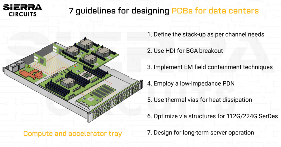
How to design circuit boards for AI-driven technologies
Standard electronics typically rely on 4-8-layer PCBs with moderate speed requirements. On the other hand, artificial intelligence models run on platforms such as NVIDIA H100/A100 GPUs, AMD MI300X accelerators, Google TPU modules, and custom PCIe or SXM-based AI cards.
These chips demand high-speed, high-density, and thermally robust circuit boards built using advanced materials. Such AI circuit boards must support on-device AI processing to handle real-time data with low latency and without cloud-based computation. They are used in a wide range of products, including autonomous vehicles, smart cameras, robotics, and other edge computing applications.
Here are the 6 best design practices:
1. Use higher layer counts to enable dense routing
AI accelerator boards often use 16 to 28 layers, far more than a typical computing PCB. This higher layer count is necessary to handle the board’s complexity, such as:
- Breaking out thousands of pins from large BGA packages
- Routing high-speed signals between GPUs/TPUs and the server architecture
- Providing multiple ground and power planes for clean, stable return paths
- Separating critical PCB interfaces like PCIe, NVLink, and high-speed memory

Stack-up design must ensure tight impedance control across differential pairs and maintain signal integrity at data rates exceeding 30–50+ Gb/s.
2. Prefer low-loss materials for multi-GHz operation
AI circuit boards cannot use standard FR4 as their dielectric losses are too high. Instead, they rely on premium high-speed laminates such as:
- Megtron 6/Megtron 7
- Panasonic R-5785(G)
- Tachyon 100G
These materials offer:
- Tg above 200°C for thermal robustness
- Low Dk (3.2–3.7) for stable signal propagation
- Ultra-low Df (0.002–0.005) for minimal insertion loss
When AI boards operate at GHz speeds, even slight loss or delay variations can degrade performance. Hence, PCB material becomes a critical contributor.
3. Adopt HDI technology
Modern AI accelerators are typically packaged in extremely dense BGA arrays with thousands of micro-bumps and solder balls. Escape routing from these packages is impossible using through-hole vias.
As a result, AI boards demand advanced HDI capabilities that include:
- Sequential lamination
- Microvias, blind vias, buried vias
- Via-in-pad plated over (VIPPO) for stable GPU/TPU mounting

When designing high-density boards, efficient signal routing is essential to achieve a compact form factor without compromising performance. For routing tips, see 5 HDI PCB routing challenges and ways to mitigate them.
HDI enables the fan-out of the dense pin fields while maintaining short via stubs, tight impedance control, and compact routing channels.
Sierra Circuits fabricates and assembles reliable high-density circuit boards with blind, buried, and microvias, ensuring excellent signal integrity.
To learn more, check our HDI PCB manufacturing capabilities.
4. Optimize the PDN to withstand 350–700W
Artificial intelligence systems draw unprecedented amounts of power, often between 350W and 700W per GPU/TPU. This requires significantly more robust power delivery than computer boards.
Key PCB design considerations include:
- Multiple thick copper power planes for low impedance
- Complex power distribution network (PDN) structures
- High-current voltage regulator module (VRM) arrays positioned close to the accelerator package
- Optimized thermal distribution to prevent hotspots

Even slight voltage drops can destabilize the system.
5. Implement high-speed signaling for PCIe, NVLink, and HBM
AI accelerators communicate using some of the fastest electrical interfaces. Typical signaling technologies include:

- PCIe Gen4/Gen5/Gen6 lanes for host connectivity
- NVLink high-speed links for GPU-to-GPU communication
- High-bandwidth memory (HBM) interfaces for extreme memory throughput
These interfaces require:
- Differential pairs routed with ±2 mil tolerance
- Controlled impedance environments
- Minimized crosstalk and insertion loss
For more details, download the High-Speed PCB Design Guide.

High-Speed PCB Design Guide
8 Chapters - 115 Pages - 150 Minute ReadWhat's Inside:
- Explanations of signal integrity issues
- Understanding transmission lines and controlled impedance
- Selection process of high-speed PCB materials
- High-speed layout guidelines
Download Now
6. Implement effective thermal management strategies
To manage such thermal density, AI circuit boards must incorporate:

- Integrated heatsinks and vapor chambers
- High-temperature solder materials
- Reinforced cores to prevent warping during reflow or operation
Thermal reliability is a defining factor of longevity and performance consistency.
Artificial intelligence is reshaping the way circuit boards are designed and built. It streamlines schematics, routing, simulation, and manufacturability checks.
At the same time, the systems that run modern AI models, such as GPUs, TPUs, and custom accelerators, demand an entirely different class of PCB technology. These include multi-layer, high-density, high-speed, thermally reinforced boards built using premium low-loss materials.
About the technical reviewer:
Abhishek Chari is the Team Lead for PCB Design at Sierra Circuits, with 6 years of experience specializing in high-speed PCB layouts and advanced HDI technologies. He possesses deep expertise in leading EDA tools, including Altium Designer, Cadence Allegro, Eagle PCB, and KiCAD.
Need help with your PCB design? Post your queries on our forum, SierraConnect. Our experts will answer them.

About Sushmitha V : Sushmitha V has a master's degree in power electronics and has over four years of experience in the PCB industry. Her areas of interest include circuit board manufacturing, assembly, IPC standards, and DFM/DFA practices.


Start the discussion at sierraconnect.protoexpress.com