


Contents

On-demand webinar
How Good is My Shield? An Introduction to Transfer Impedance and Shielding Effectiveness
by Karen Burnham
Automotive PCBs have gained popularity due to the ongoing race between car manufacturers to capture market share. Electric or ICE, circuit boards are an essential part of almost every automobile. Advancement of these boards has enabled manufacturers to integrate revolutionary features such as autopilot, automatic parking, emergency braking, keyless start, and lane assistance into modern-day vehicles.
In this article, we will talk about 10 automotive PCB design guidelines that can help you create an efficient device. Before that, here’s a quick overview of automotive boards.
What is the role of circuit boards in automotive?

Components like automotive sensors, GPS modules, illumination systems, door switch modules, engine control modules, and audio systems are held together by circuit boards. Hence, the entire operating mechanism of the vehicle depends on the board design and layout. Automotive PCBs have led to significant developments, such as:
- Improved performance in terms of fuel efficiency.
- A reliable safety and security system that reduces traffic accidents. You can find the visibility of printed circuit boards in systems like airbags, radar monitoring, stereo cameras, and infrared monitoring.
- The strategic evolvement of eco-friendly applications. This has led to the production of electric vehicles and driverless vehicles.
To learn how the PCBs in your EV support battery management, power distribution, and vehicle control, see what kinds of PCBs power electric vehicles?
10 guidelines for automotive PCB design
Your board must meet the specifications outlined by relevant standards. Pursuing a meticulous design process will prevent problems during production. To make your design more viable, adhere to the following important guidelines:
1. Component orientation and placement
The positioning and orientation of components have a substantial impact on a board’s dependability, manufacturability, and performance. You can analyze the board for any upgrading and defect detection by organizing and differentiating the components. Follow these approaches while placing the components:
- Place similar components in the same direction. This will facilitate routing and soldering operations during assembly.
- For wave soldering, the components should be in parallel to the direction of the wave. This will avoid solder bridging or open circuits.
- Provide a large space between the inductors on your board.
- Align the inductors at right angles to each other. This will reduce crosstalk.
- Place the large and most significant components first.
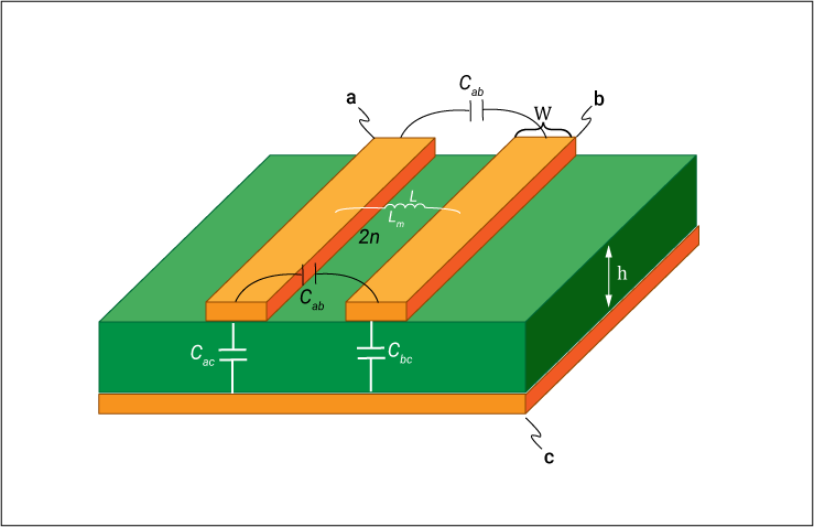
- Separate the analog and digital components into different sections of the board.
- Avoid arranging tall components (such as electrolytic capacitors) adjacent to shorter ones. This will prevent loose solder junctions.
- Keep the high-power components as far as possible from other components to optimize the heat dissipation on your board.
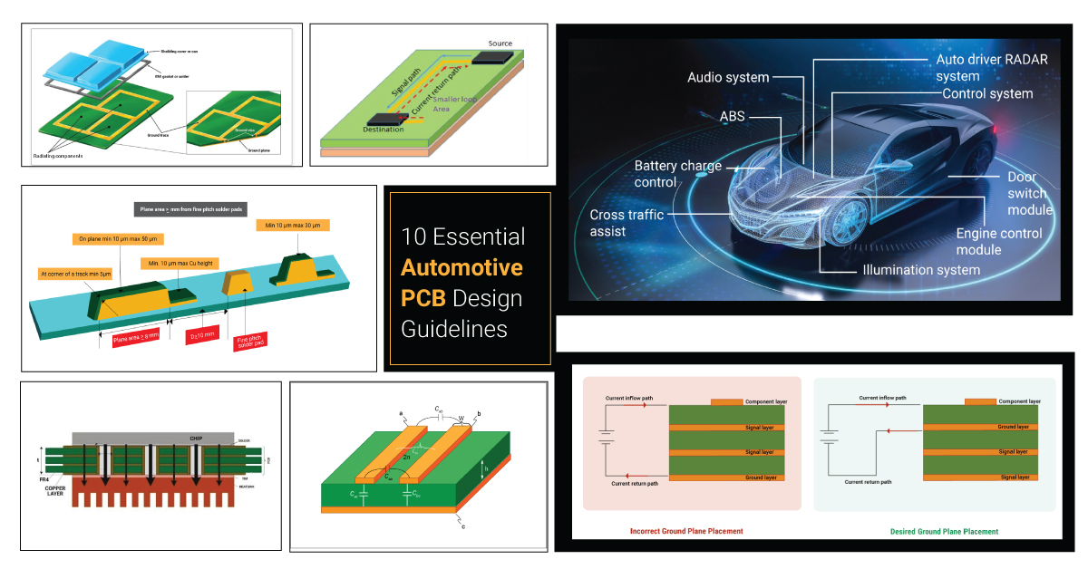
2. Lead placement to prevent coupling
The improper placing of leads can affect the magnetic coupling, and mutual inductance may be produced. Consider the below-listed guidelines for effective lead placement:
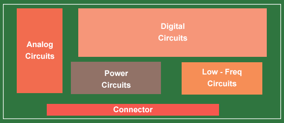
- Avoid placing the leads close to each other.
- Choose the return current path near the main current path in an area with little radiation. With this, you can reduce the current loop area.
- Implement a holistic grounding under the leads. This will increase the board’s performance.
3. Signal routing in automotive PCBs
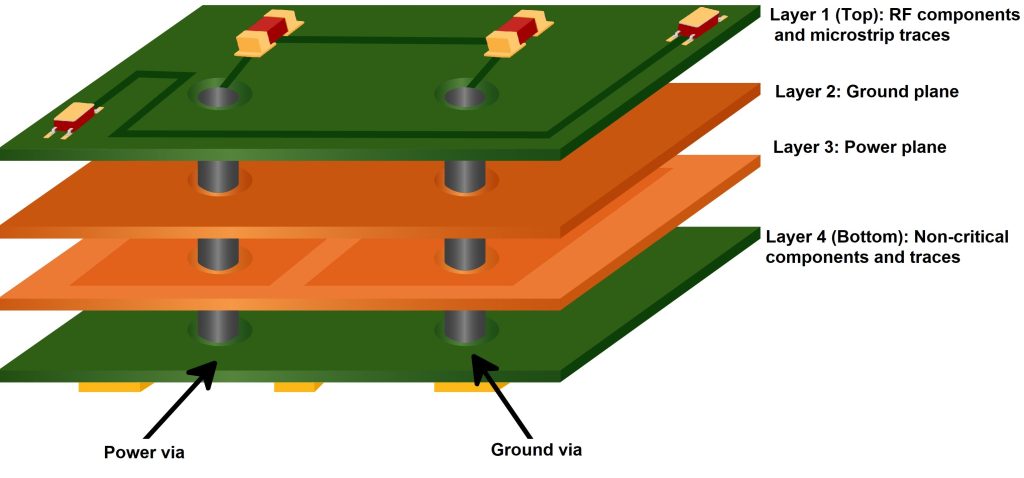
Use two to four vias per layer to connect layers that are conducting high currents. This will increase reliability, decrease resistive and inductive losses, and improve thermal conductivity. Stick to the following automotive PCB design guidelines for signal routing:
- Place the power and ground planes on the inner layers.
- Protect sensitive signals from noise sources with planes and ensure a controlled impedance for their transmission.
- Adapt the shortest and straightest tracks possible for routing.
- Route the traces horizontally on one side, and vertically on the other side for a dual-layer circuit board.
- Arrange the vertical and horizontal traces alternately for a multilayer board.

Signal Integrity eBook
6 Chapters - 53 Pages - 60 Minute ReadWhat's Inside:
- Impedance discontinuities
- Crosstalk
- Reflections, ringing, overshoot and undershoot
- Via stubs
Download Now
4. Effective thermal management
Follow appropriate thermal management techniques to dissipate heat for components that absorb more than 10 mW or conduct more than 10 mA. Employ the points below for better temperature control:
- Select the copper planes and signal vias as thermal vias to increase thermal conductivity.
- Locate the signal vias closer to the components with surface pins or right below SMDs.
- Provide heatsinks for high-power components.
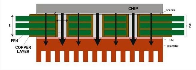
Heat sink for high-power-components
- Place metal thermal pads under the hot parts of the board.
- Solid-filled vias can be used to transfer heat from thermal pads to ground planes.
- Use a metal core or polyimide for the board, as they have improved thermal characteristics.
- Employ multiple ground and power planes and directly couple them to the heat sources through thermal vias. This can reduce the operating temperature.
- Prefer high Tg boards as the operating environment tends to heat up the PCB frequently.

5. Perform frequent design rule checks
Run design rule check to find any errors that might not meet general manufacturing and high-speed requirements specific to your application. A general DRC must:
- Check for the appropriate spacing between components for the entire circuit board and individual layers.
- Spacing between the power supply and ground wires. Provide a wide space for ground lines.
- Check for proper ground connections for analog and digital circuits.
- Suggest modifying undesired lines, such as open-ended stubs.
- Verify whether the layout connectivity matches the schematic diagram’s defined connectivity.
- Analyze if the outer rim of the power layer is reduced. This will avoid short circuits when the power layer is exposed.
- Verify signal integrity, power integrity, electromagnetic interference, and safety checks
6. Incorporate automotive design standards
A complex and compact board will assist you in running the infotainment systems, communications, safety, driver-assistance systems, the engine, and the power train. The complexity of PCB design for automotive will increase as the technology quickly develops toward more advanced driverless cars. Therefore, for a durable automotive design, adhere to the standards specified by IATF 16949, IPC- 6012 class 3, AEC-Q100, and SAE J3016_201401.
IPC-6012
IPC-6012 mainly provides guidelines for automotive PCB design in terms of pattern, solder mask thickness, copper thickness, and other parameters related to manufacturing. Follow the specifications as listed below:
- Keep the hole’s position accuracy within the limits. The allowed tolerance is 100 microns.
- Via holes shall be specified as the minimum drill size to secure a sufficient aspect ratio.
- Maintain a minimum drill hole size to achieve a good aspect ratio.
- Ensure the hole wall separation is not more than 40% of the dielectric thickness.
- Maintain cleanliness before the solder mask application. Contamination level can be up to 0.75 g/cm2 sodium chloride equivalent.
- Perform preconditioning before you assess the board for bow and twist. This is according to IPC-TM-650. Preconditioning is done after the soldering process to determine the cracks, opens, and short circuits.
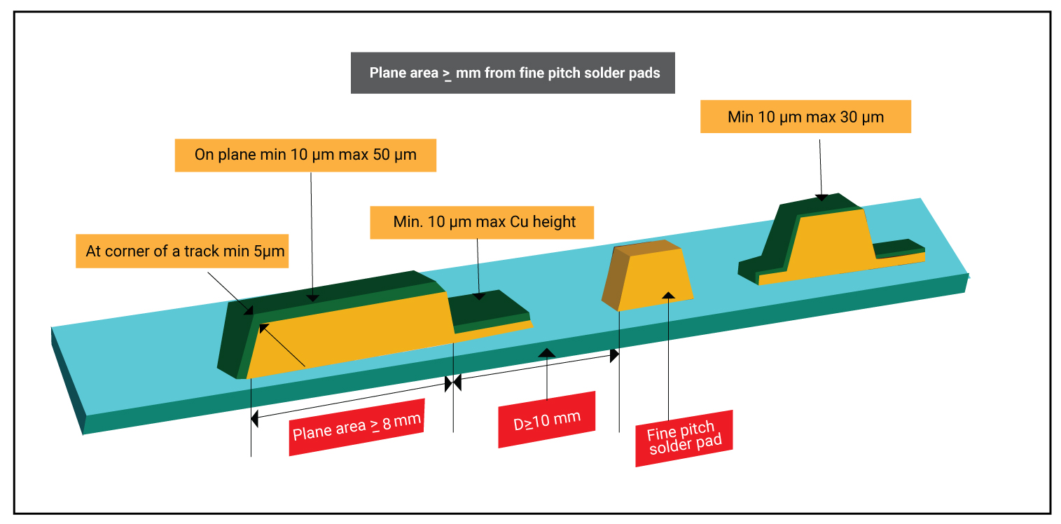
- Inspect solder mask parameters to ensure they adhere to IPC-6012FA. For instance, if you are using a board of class 3 copper plating and 18 µm base copper thickness, the allowed solder mask thickness is mentioned in the table below:
| Region | Solder mask thickness |
| Conductor adjacent to surface mount pads | 5 µm minimum 30 µm maximum |
| Ground planes | 10 µm minimum 60 µm maximum |
Class 3 would be the best option if the board is required to handle a crucial application and is anticipated to last for more than 15 years. To make class 3 boards highly reliable, here are a few pointers:
- Design your PTH 15 mils over the diameter of the lead. The amount of barrel fill required for through-hole leads is 75%.
- The minimum internal annular ring should not be less than 1 mil, and the external annular ring should not be less than 2 mil.
- Stick to the specified pattern tolerances. The acceptable tolerance for a board of dimensions up to 300 mm is +/- 75 µm, up to 450 mm is +/- 112 µm, and up to 600 mm is +/- 150 µm.
| Drill | Pad | Anti-pad | PCB thickness | Aspect ratio |
| 0.008" | 0.023" | 0.033" | Upto 0.062" | 7.75:1 |
| 0.010" | 0.025" | 0.035" | Upto 0.100" | 10:01 |
| 0.012" | 0.027" | 0.037" | Upto 0.120" | 10:01 |
| 0.0135" | 0.028" | 0.038" | Upto 0.135" | 10:01 |
For a better understanding, download our Class 3 Design Guide.

IPC Class 3 Design Guide
8 Chapters - 23 Pages - 35 Minute ReadWhat's Inside:
- IPC guidelines for manufacturing defects
- IPC standards for assembly processes
- Common differences between the classes
- IPC documents to set the level of acceptance criteria
Download Now
7. Grounding through-hole mounting holes
The mounting holes should be plated and grounded. The poor impedance of various circuits is one of the problems. This is mainly due to various electronic components and their connectivity. Therefore, the following guidelines can be employed for automobile designs:
- Place the inductance module in sensitive areas close to the through-holes.
- Use appropriate filter networks as they depend on through-holes.
- Make the copper on the layers thinner. This will reduce the impact of through-hole parasitic inductance.
8. Optimize the RF circuit
PCB design for automotive ideally incorporates RF circuits. This can be challenging for you to address issues related to coexistence, power consumption, and long-term reliability. Incorporate the below-mentioned tips in your design:
- Use extremely linear active or front-end devices.
- Pay attention to the radio frequency front-end control efficiency, current use, and power dissipation.
- Select a high-performance RF filter to reduce the insertion loss, temperature drift, and interference.
- Use components that combine transmit, receive, and filtering capabilities into a single unit.
9. Adapt good grounding techniques
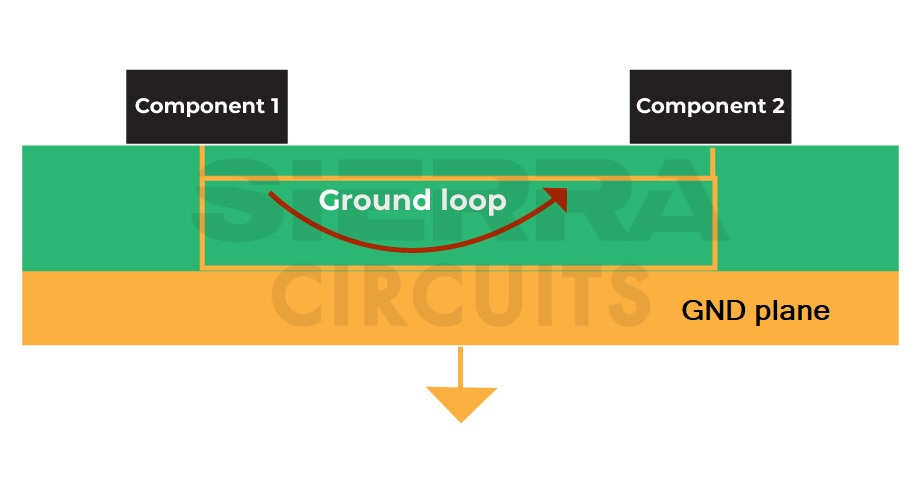
While planning grounding techniques for your automotive design:
- Create a single-point ground connection for each automotive board.
- Provide a continuous grounding region with extremely low impedance.
- Connect the ground to the filling wire terminals with the thru-hole array.
- Always connect the copper-coated cables to the ground.
10. Prevent electromagnetic interference in your automotive PCB design
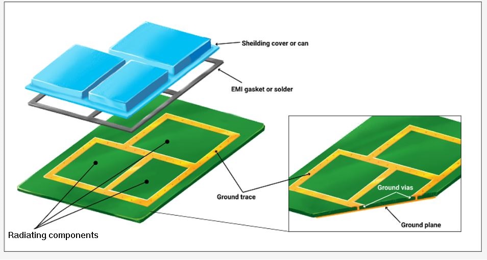
In any circuit, it is vital to adopt preventive measures to limit EMI. This will ensure the smooth operation of the automobile. You can protect your board from the effects of magnetic interferences by incorporating the listed measures:
- Keep the effective area of the loop minimum.
- Provide magnetic shielding for the board and the components prone to causing interference.
- Use differential pairs to transmit signals in the circuit.
- You can reduce network interference by using rational lead routing.
- Increase the power filtering capacitance and add an RC decoupling circuit.
- Use distributorless ignition to eliminate interference sources and lower electromagnetic radiation.
- Employ CAN bus protocol to reduce heavy wiring and thus minimize the effect of electrical disturbances and EMI.
Need help in designing reliable PCBs? Our engineering team can help you with thermal management, stack-up design, and DFM analysis.
You can book a meeting with our experts or call us at +1 (800) 763-7503.

Different types of boards in automobiles
Rigid boards: They are made up of solid laminates like FR4, Rogers, etc. You can find rigid circuit boards on display monitors and rear-view cameras.
Flex circuits: They have a flexible substrate for mounting electronic components. Flex circuits can be bent and twisted, hence employed in bends and corners. Flex PCBs are used in a car stereo and monitoring system.
Rigid-flex: These boards allow you to utilize both the aforementioned technologies in a single board. They find their prominent application in lighting systems.
LED PCB: In modern automobiles, high-power and high-brightness LEDs require circuits with great heat dissipation. Such boards are built from a metal substrate like aluminum. They are part of automotive brakes, headlights, and indicator lights.
Heavy copper: The outer and inner layers of such boards contain three or more ounces of copper. They are found in a vehicle’s safety and signaling system.
Based on the applications, you can also choose metal core, multilayer, double-sided, or single-sided boards.
Modern automobiles are built with sophisticated boards to control the engine, fuel efficiency, auto-drive systems, and more. Your board must be optimized to meet the specifications related to pattern features, thermal control, and signal integrity. The guidelines mentioned in the blog post will certainly help you in creating a robust design.
If you have any queries related to automotive PCB design, please post them on our forum, SierraConnect. We will be happy to help you.


