


Contents
Before we start with today’s article, something needs to get engraved in your mind. If some current goes out somewhere, it will always return to the source, with no exceptions. Hence, there is always a current loop, a current return path, along with the current-carrying traces.
So, the current does not care if you provide that return path. It will find its own. But if you do not, it will interfere and mess around with your entire circuit while finding its way back.
Highlights:
To ensure efficient return paths:
- Route low-frequency return currents along the path of least resistance and high-frequency return currents along the path of least inductance.
- Implement solid ground planes under signal traces to minimize loop area and inductance.
- Avoid ground plane discontinuities such as slots, cutouts, or overlapping clearance holes to prevent current loops and noise.
Common challenges PCB designers face when routing high-speed and RF traces
In our recent webinar, resolving common errors in RF PCB layout design, we surveyed 30 PCB designers, out of which 43.3% of respondents reported difficulties in managing return paths and grounding requirements.

In this article, you’ll learn the strategies for designing efficient current return paths. To learn how to design a stable ground, see best PCB grounding techniques for high-power and HDI designs.
What is a current return path?
The return path of current is nothing but the path it follows while returning to the source. Do you remember what an electrical circuit is? It is a path through which electrons flow from a voltage or current source. The ‘source’ of electrons is the point where they enter into the circuit. And the point where electrons leave an electrical circuit is called the ‘return’ or ‘ground.’ Since electrons always end up at the source when they complete the path of their circuit, we call that exit point ‘return.’
Why does the current return?
The current return because to the charge and energy conservation principle. Suppose the current does not return to the source. Then what? The charge will still build up at someplace. There will be an excess of (+) charge at a place and an excess of (-) charge somewhere else. That disturbance would cause potential differences that would, in turn, make the current flow backward. Do you remember Kirchhoff’s Law (the 1st law)?

Signal Integrity eBook
6 Chapters - 53 Pages - 60 Minute ReadWhat's Inside:
- Impedance discontinuities
- Crosstalk
- Reflections, ringing, overshoot and undershoot
- Via stubs
Download Now
Kirchhoff’s current law states that the current entering into a node (or a junction) must be equal to the current flowing out of it. In other words, the algebraic sum of all the currents entering and leaving a node must be equal to zero such as:
I(exiting) + I(entering) = 0
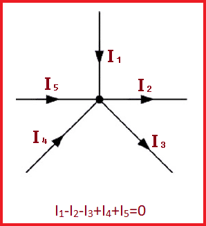
Therefore, the net flow of charge in and out of every node and component in a circuit should be zero. It implies the current must return to its source, no matter what the circuit is. For a better understanding, read our post on network theory for better PCB design and development.
If the current flows in loops and returns to the source, you would expect the current to travel to the end of the line and flow back down the return path. But how long does this entire process take? When can you see the current come out of the return path? Does it take two seconds? Or, one second to go down and one second to come back? Suppose there is an insulating dielectric material between the signal and return conductors. How could the current possibly get from the signal to the return conductor, except at the far end?
Let’s start by thinking in the basic model, the line through which the current flows, let that be a bunch of tiny capacitors. The initial current flows into the line. As the signal launches, it sees the capacitor. If the voltage across the capacitor is constant, the current will not flow. As the signal enters the transmission line, there is a voltage build-up across the signal and return path. During this transition time, as the edge passes, the voltage changes, and the current flows through the initial capacitor. When the signal is launched, it has no idea how you have planned its entire trip, and it does not matter. The to and fro motion of the current depends on the immediate environment and the region of the line where the voltage is changing, i.e., where the signal edge is.
To learn more about transients, see Transient Analysis for Non-Sinusoidal Signals.
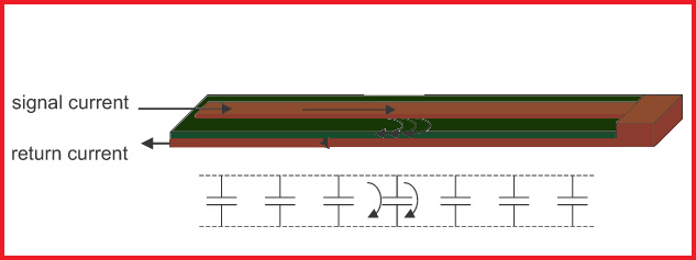
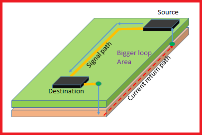
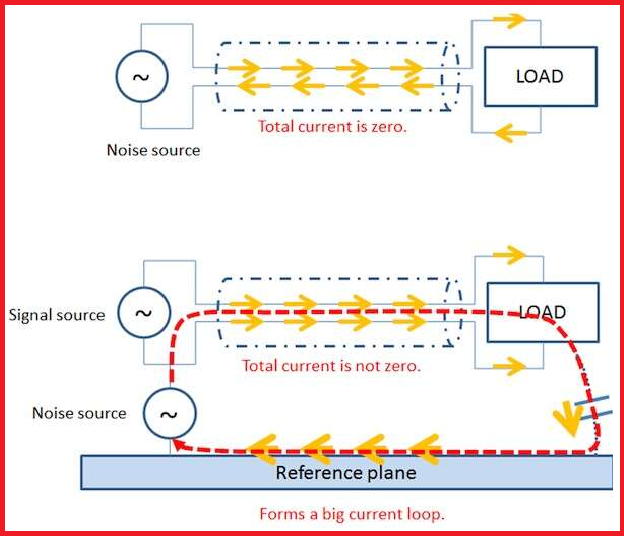
The source current flows into the conductor and passes through the capacitor between the signal and return path, forming a loop. As the voltage transition edge propagates through the line, the current loop also propagates through the transmission line. We can extend the transmission line model to include the rest of the signal and return paths with all distributed capacitors between them, provided the signal voltage is changing.
Anything that disrupts the current loop will disrupt the signal and distort the controlled impedance, compromising signal integrity.
Routing the current return path deliberately!
Many people imagine changes in a circuit occur immediately, as you switch on a circuit and the light shines in just a click. It is relatively easy to have a misconception because the change in the state exceeds human perception.
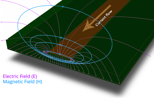
But in reality, when an ‘alternating current’ passes through the circuit, it sets up an electric field in its vicinity. These field lines will then spread through the surrounding conductors and may transfer to nearby circuits as well. Along with this, your circuit faces a change of state that in turn gives rise to an electric potential, and hence the current passes through the circuit. This electric field generates an electromagnetic field around the conductor through which the current is passing.
Changes in the electromagnetic field propagate very fast but at a finite speed, and it takes some time for the changes in the field to reach the far ends of your circuit. Therefore, it is possible for two ends of a trace to be in two different states, with a transition point that moves along the length. This will give rise to unwanted currents in nearby conductors.
Poor routing can lead to noise in the circuit and can create issues such as electromagnetic compatibility, susceptibility, and create electromagnetic interference. Hence, degrading the overall circuit performance.
Why is the current return path vital in a PCB design?
Yesteryear’s electronic design was kind of considerate. Somewhat bad schematics and not so efficient layout would still produce some meaningful and functional boards. But now, in the race to make PCBs and chips smaller, the operating voltages and their noise margins are getting reduced. The reduction is so that the engineers now need to be extra mindful in their design choices.
Not only smaller, but PCBs are now getting faster. Now, PCBs are intended to operate at frequencies high enough to degrade the circuit’s performance significantly. Those are called high-speed PCBs. Other factors include the materials, the length of the traces, the size of the board, and the environment.
Though, traditionally, 50MHz and above are the points where a PCB layout can be considered a high-speed PCB design. The interesting aspect of high-speed PCBs is that they don’t follow the least resistance path; they follow the path of least impedance. Without a proper return path layout, you might find yourself with currents spreading around splits in your ground plane, leading to a loss of signal integrity. Use of dedicated ground planes and implementing ground via stitching are a few of the best grounding techniques used in high-power/HDI boards.

High-speed PCBs and current return path
No matter how much experience you have, you could forget that impedance may look like resistance. But it’s not. It is a generic expression that accounts for time and frequency dependency. It is a complex quantity with an imaginary (reactance) part and a real (resistive) part.
So, you may tend to ignore the reactive part of impedance in your circuit return paths and focus strictly on the resistive. With the increase in frequency and depreciation in rise/fall time, the reactive part of impedance becomes more critical in return paths.
In some cases, the return path of the current can be found underneath the conductor. Therefore, you should provide a desirable path before a less desirable path is established in your circuit.
Now, let’s go ahead with how a high-speed PCB current return routing is done.
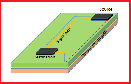
Suppose you have a double-sided board, a single trace on top, and a full copper ground plane at the bottom. The board has two vias that connect the trace with the ground plane. Upon reaching its desired point, it travels to the ground plane through the via and ends up at its source again through the via.
But the question here is how? The current can return in three given paths: the easiest known path is to trace back its flow, the direct path. Or, it can travel in the least area loop which is underneath the top trace. Otherwise, it can combine both ways to travel back to its source. As you already know by now, current returns to the source through the least impedance path.
We know that the impedance (Z) of a resistor equals the value of the resistor (R), such as:
Z = R
Again, the magnitude of the impedance in an inductor is:
|Z| = ω.L
In the frequency domain, we can express the impedance of an inductor as:
Z = j.ω.L
Therefore, using the lumped-parameter circuit theory, we can find the ground impedance Zg.
Zg = Rg + jωLg
Where Rg and Lg are the ground path resistance and inductance, respectively.
For low frequencies, the ground current takes up the path of least resistance. It traces back the path to the source, the lowest impedance path.
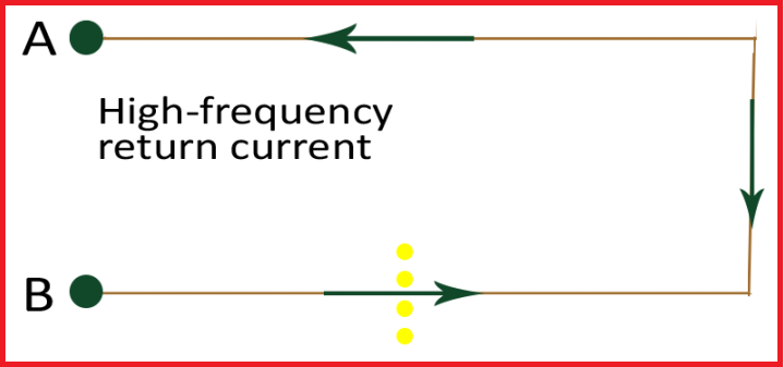
For high frequencies, the ground current will follow the route of least inductance. This is directly underneath the trace because it represents the smallest loop area. Read our post on the effects of high-speed signals in a PCB.
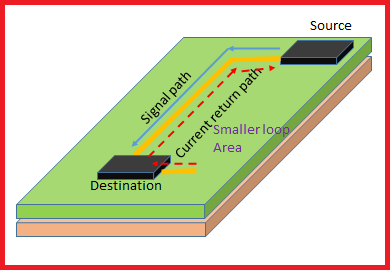
At low frequencies (1 – 100kHz), the return current flows mainly through the direct path of the least resistance. As the frequency increases to 500 – 1000kHz, the current splits between the two paths of the least resistance and least inductance. At high frequencies (10 – 100MHz), the majority of the return current flows underneath the top trace through the path of least inductance.
For higher-frequency signal traces, a differential pair is used. The reason for this is simple: the differential pairs carry both the signal and the opposite phase of the signal. Hence, the radiations get canceled, and the current flowing is zero. Therefore, they can combat common-mode noise or induced noise. Careful and deliberate planning of a ground return path will keep unwanted currents from forming in parts of your circuit where they should not be.
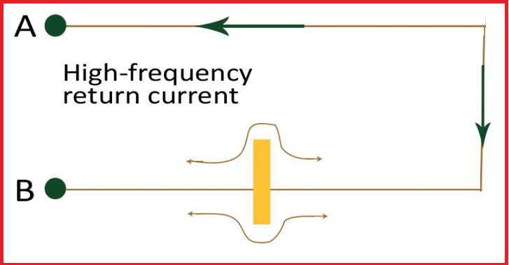
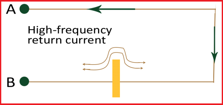
Current return path discontinuities
Until now, whatever we discussed were the cases of a solid ground plane. But there can be situations where there is a discontinuity in the ground plane. While designing for return paths, you should also keep in mind cases of cutouts, slots, or maybe clearance holes. Suppose there is a slot in the ground plane; what do you think can go wrong?
This is conventional that a solid and uninterrupted return path would have a better electromagnetic capability. The current would go along a closed-circuit loop, hence making the resultant current zero. The loop is small/narrow enough; the return path of the via microstrip is just beneath the plane of a signal trace.
But discontinuities in the return path will give rise to noise. Cutouts, slots, or even clearance holes for through-hole or vias can cause a discontinuity in the return path. It creates a larger current loop area. This increases the loop inductance. Hence, the current will spread out and might also get to the edges, forming an antenna. The clearance holes are less of a threat to the current flow. Unless the holes overlap, there is not much of an issue. Read how to limit impedance discontinuities and signal reflections in a PCB transmission line.
Everything that affects the signal current or the return current path will affect the impedance of the signal. Therefore, the return path should be designed just as carefully as the signal path. It does not matter if it is on a PCB or an IC package. Return paths also play an important role in assembling connectors and cables.
Current return path in mixed signal boards

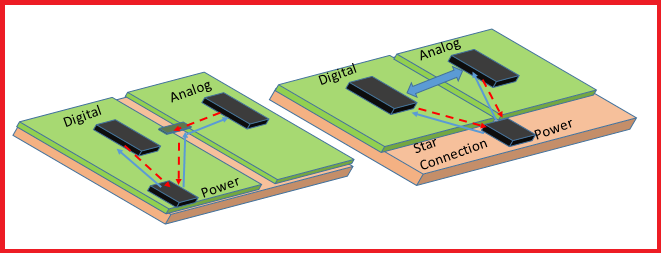
In mixed-signal boards, it is imperative to plan the component placement so that analog and digital signals do not cross each other. Refer to the above image (left) for the return path of an analog signal. In this case, we see that the board area is split into the digital and analog sections, and both sections are interconnected in the bottom ground plane stitching at the center. The two planes will still experience capacitive coupling, allowing analog and digital signals to mix. The best approach is to have a single plane, as shown in the image (right), and place the digital and analog components separately. The motive is to prevent the digital signals from traveling beneath the analog region and causing interference.
Key takeaways:
- Always provide continuous return paths to prevent currents from spreading unpredictably across the PCB.
- Use solid, uninterrupted ground planes directly under high-speed traces to ensure minimal inductance.
- At higher frequencies, prioritize return paths directly under the signal to avoid EMI and maintain impedance control.
- Avoid ground plane discontinuities that enlarge loop areas and act as unintentional antennas.
- Use differential pair routing for high-frequency signals to minimize radiation and noise susceptibility.
- In mixed-signal designs, isolate analog and digital return paths through careful component placement and plane management.
Trace geometry and internal planes critically determine the current return path in a PCB layout. A properly planned and carefully designed current return path is critical to avoid unwanted current in a circuit. It is advised to provide ground return vias and paths for all the high-speed signals passing through the circuit. Once a designer understands the geometry and the characteristics of a signal, it becomes easier to plan the return path for signals.
Have questions on your PCB design? Post them on our forum, SierraConnect. Our design experts will answer them.


