


Contents
Power integrity is one of the mind-boggling subjects when it comes to PCB designing. In this blog, we have tried to explain everything related to power integrity.
What is power integrity?
A circuit board requires one or more power supply voltages to operate. These are mostly generated by Voltage Regulator Modules (VRMs). These VRMs are designed to deliver the required maximum currents at the required voltages to the various devices on the circuit board.
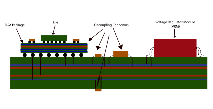
The Power Distribution Network (PDN) consists of all the interconnects from the VRMs to the terminals/pads of various components and devices (ICs, etc.), including all the bulk and ceramic decoupling capacitors, power and ground planes, the intervening vias, traces, and the relevant leads, solder balls, wire-bonds, etc. of the device packages.
A PDN’s voltage rail is a single net but a very large one, having many components connected to it, and is spread over almost the entire PCB. PDN is susceptible to electrical noise generated by the components and the various signal, power, and ground nets on the PCB. Furthermore, the faster and greater the number of signal transitions (rise and fall times) switching over various I/Os and internal circuits of the devices on the board, the greater the magnitude and frequency bandwidth of the electrical noise on the PDN.
PDN noise is injurious to the proper functioning of the board in several ways:
- When the magnitude of the noise on PDN exceeds a certain threshold, it alters the voltages delivered to the ICs below the acceptable values, causing malfunction of the circuits on the board.
- Even if a PDN supplies a voltage to the devices within tolerance, the PDN noise may cause other problems. It can cause or appear as crosstalk on signal lines; it can transfer to the input power source line, from where it can pass on to other VRMs inputs, thereby to their outputs.
- Furthermore, as PDN interconnects are usually the largest conducting surfaces on the PCB and carry the highest currents, any high-frequency PDN noise can create a lot of electromagnetic radiation, possibly causing failure to pass EMC compliance.
It is therefore important to control the PDN noise and ensure that it delivers the required voltages within acceptable tolerance limits (usually within ± 2 to 5%), across the power supply voltage and ground terminals of the various devices mounted on the PCB, and the devices’ dynamic current demands are met at all times and over their entire functional frequency range.
Power Integrity (PI) deals with all aspects of the PDN – it is designed to control the PDN noise.
Read our blog 5 typical PCB design challenges with solutions for engineers to learn common prototyping issues and strategies to resolve them.
Power distribution network (PDN) block diagram
Before we analyze the PDN in greater detail, let us look at a general PDN:
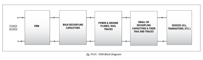
PDN starts from the various VRMs followed by bulk decoupling capacitors (usually electrolytic – aluminum/tantalum/polymer), power and ground planes with associated via and traces interconnects, multiple HF decoupling chip capacitors (usually ceramic capacitors) and the associated vias and traces interconnects to power supply voltage and ground pins of the various Devices – ICs, transistors, etc.
Also read: 7 Considerations for PCB Power Supply Design
What is PDN noise?
The control of PDN noise plays the most important role in ensuring good power integrity. To control it, one must first understand and analyze the causes and sources of the PDN noise.
If there were only constant DC flow in the PDN interconnects from the VRMs to the ICs, that would cause a constant voltage drop, called the IR Drop, between the VRM and the ICs:
IR Drop = (Series resistance of the power and ground rails) X (Current in the rails) ……………… (PI-1)
However, the current drawn by the ICs and devices on the board is never constant but fluctuates rapidly with time. Thus, the current drawn is not DC but an AC current, and instead of ‘IR’ drop, we will need to consider the ‘IZ’ drop where Z is the AC impedance of the PDN network:
AC Voltage on PDN = (AC Impedance of the PDN) X (AC in the PDN) …………………….. (PI-2)
In ICs and transistors, when the digital signals, either inside the IC chip and/or on the I/O pins and associated circuitry, switch from one logic level to the other logic level, the current drawn from the power supply pins of these devices also changes.
This change occurs in a very short time characterized by the rise or fall time ‘tr’ which ranges from sub-nanoseconds to a few nanoseconds in high-speed circuits.

High-Speed PCB Design Guide
8 Chapters - 115 Pages - 150 Minute ReadWhat's Inside:
- Explanations of signal integrity issues
- Understanding transmission lines and controlled impedance
- Selection process of high-speed PCB materials
- High-speed layout guidelines
Download Now
If ΔI is the amount of change in the current drawn by the IC from the power supply, and Δt = tris the time during which this change occurs. This change will induce a voltage Vnoise= L x (ΔI / ΔT) = L x (ΔI/ tr) across the power and ground pins, where ‘L’ is the inductance of the loop formed by the path of the power and ground nets i.e. the PDN.
This noise voltage is rightly a cause of the PDN noise. There are three things apparent from this PDN noise source:
- The greater the ΔI is, the greater will the noise voltage be. So, if multiple signals say ‘n’, are switching simultaneously in one or more devices on the same power rail, the current change in time ‘tr’ on that rail will be nΔI, so that noise voltage will become ‘n’ times:
VnoisePDN = L x n x (ΔI/ tr) ……………………………………………………………………… (PI-3)
Complex ICs – FPGAs, microcontrollers, memories, ASICs, etc. – (i) have many I/Os and (ii) quite a lot of internal processing inside them as per programs running therein.
Both these sources result in switching taking place in a tremendous amount, and it would be very likely that a large number of signals are switching simultaneously, resulting in a large magnitude of PDN noise.
- The smaller the value of ‘tr’, the greater the value of PDN noise. In our present era of ever increasing processing power occurring in shorter and shorter time durations in complex ICs and transistors, we are confronted with very high data transfer rates and extremely small rise times i.e. ‘tr’ – in the range of few tens of picoseconds. Obviously, these devices have the potential to create very high PDN noise.
- Finally, the greater the PDN inductance ‘L’ is, the greater the PDN noise will be. What contributes to ‘L’ in the power delivery path? There are many sources:
-
- Firstly, every loop in the PDN interconnect has a parasitic inductance proportional to its loop area. Thus, all the interconnects – inside the IC chip, from inside to IC terminals, from IC terminals to PCB pads, PCB traces, and vias from pads to decoupling caps to power and ground planes and then to the VRMs – all form the current path loops with inductances (usually in nH range).
- Secondly, the decoupling capacitors – bulk electrolytic and ceramic types – are not ideal. They have inductances associated with their external and internal leads called ESL- the Equivalent Series Inductance – which can be several 10nHs in the case of electrolytic capacitors and a few nHs in the case of ceramic capacitors. Capacitors also have ESR – Equivalent Series Resistance – drop-through, which adds to the PDN noise. The equivalent circuit of a real capacitor of stated value C is shown in the following diagram.

The capacitor’s inductance increases its impedance at higher frequencies where it no longer functions as a capacitor. Every piece of conductor on the PCB and inside the components in the power delivery path has some parasitic inductance associated with it.
If we look at equation (PI-3), given the ICs and other active devices on the circuit board, the only thing in our control to limit the PDN noise is the PDN inductance L!
Read 4 common PDN design challenges and how to resolve them for ways to mitigate PDN noise.
Analysis and design of PDN
A circuit schematic diagram of the PDN network can be represented as follows:

The top and bottom lines represent the power and ground rails or planes. At P and G, an IC is connected. This network comprises mainly VRM, resistors, inductors, and capacitors, and its analysis is most conveniently done in the frequency domain by circuit analysis techniques, either manually or by using SPICE.
What we need is to estimate the required spectrum of the frequencies of interest and look at the impedance ZPDN of the PDN network looking back from the points P and G where the devices – ICs and transistors – are connected to the PDN, and analyze how ZPDN varies with frequency over the bandwidth of interest.
To learn how to ensure a stable PDN in a power electronics board, see 7 PCB layout design tips for power electronics.
4.1 Target impedance ZPDN and its frequency spectrum
If Imax is the maximum current consumption rating of a particular PDN voltage rail – say of VCC – then the actual current drawn by VCC rail may vary, over some time, from very low to almost Imax depending on how many and how fast I/Os are switching simultaneously at a particular instant.
If the fastest rise time is tr, then the highest frequency content in the current waveform is of the order of fm = 0.5/ tr , and it would be prudent to say that noise current waveform has a spectrum covering the frequency range from DC to fm , and the magnitude Îm of a sinusoidal current waveform at any frequency of interest in this spectrum is ≤ Îm = (1/2) Imax.
If ZPDN is the impedance of the PDN network at the frequency of interest, then the noise voltage generated on the VCC rail will have a magnitude V̂Noise given by:
V̂Noise = ZPDN x Îm ………………………………………………………………………… (PI-4)
This noise voltage will occur as ripple voltage on the VCC rail. In order for the ICs connected to the VCC rail to function properly, we need to ensure the V̂Noise magnitude does not exceed the acceptable ripple voltage of the IC’s power supply voltage VCC :
V̂Noise ≤ Acceptable voltage ripple = VCC x Acceptable Ripple% ……………………(PI-5)
Therefore, ZPDN ≤ (VCC x Ripple%) / (Îm) = (VCC x Ripple%) / (0.5 x Imax) ………………………(PI-6)
We now define the Target Impedance – ZT-PDN – of the PDN network by:
ZT-PDN = (VCC x Acceptable Ripple %) / (0.5 x Imax) …………………………………… (PI-7)
So the actual PDN impedance should be limited by:
ZPDN ≤ ZT-PDN (over the entire frequency spectrum of the PDN Noise Current)……… (PI-8)
In the picture below, we show a typical good PDN impedance plot vs frequency and the Target Impedance of the PDN. The actual impedance does not go above the target impedance line for the entire frequency range from DC to 10GHz, and that means that it meets the condition of the above equation (PI-8).
Thus, the design of a good PDN network involves the following steps:
- Determine the highest frequency fm = 0.5/ tr where tr is the fastest signal rise or fall time. DC to a few fm is the frequency range of interest.
- Calculate the target PDN impedance ZT-PDN for each voltage rail as per the above equation.
- Draw the PDN network or a simplified version of it, and calculate, using SPICE or manually, the actual PDN impedance at various frequencies i.e., to plot the PDN impedance spectrum (plot of impedance magnitude vs frequency) and to understand how various decoupling capacitors and geometry of the PCB conductors and vias in the PDN affect this spectrum shape.
- Choose appropriate decoupling capacitors and geometry of the PCB conductors and vias in the PDN to ensure that ZPDN ≤ ZT-PDN for each voltage rail over the entire frequency spectrum of interest.
Examples of calculation of fm and ZT-PDN :
(1) For VCC = 3.3V rail, Let the fastest rise time be 1ns. Therefore, the highest frequency is: fm = 0.5/ tr = 0.5/ (1 ns) = 500MHz. Let Imax = 3A, ripple = 3%. Therefore, ZT-Vcc = (3.3V x 3%) / (0.5 x 3A) = 0.066Ω
(2) For VDD = 1.2V rail, Let the fastest rise time be 0.5 ns. Therefore, the highest frequency is: fm = 0.5/ tr = 0.5/ (0.5 ns) = 1000 MHz. Let Imax = 1A, ripple = 2%. Therefore, ZT-VDD = (1.2V x 2%) / (0.5 x 1A) = 0.048Ω.
Generally, the target PDN ZT-PDN impedance falls in the range of 0.04Ω to 0.1Ω for most medium-to-complex requirements. And the frequency band of interest is DC to 1GHz. Thus, the ZPDN magnitude should not go above ZT-PDN for the entire frequency band from DC to 1GHz. See the picture below as an example:

4.2 Estimation of actual ZPDN over the bandwidth
To estimate the actual PDN impedance at various frequencies, we must analyze its equivalent circuit schematics model like the one shown in Fig. PI-03 above. The values of the resistors are quite small as compared to the impedances of inductances and capacitances; therefore, a simplified schematics of a typical PDN network can be depicted as hereunder:

If we see the impedance of the above PDN looking back from P and G, we realize that the VRM, the bulk capacitors, HF decoupling capacitors, the IC package, and the die play a very significant role in determining the magnitude of ZPDN in various frequencies zones. In PCB design, the IC package and die are not in our control, but the other elements are. We will, therefore, concentrate our analysis on the VRM, bulk capacitors, and HF decoupling capacitors and their frequency zones of influence on PDN impedance.
Also read: The Pros and Cons of Composite Amplifiers
4.2.1 Voltage Regulator Module (VRM)
At low frequencies – from DC to about a few kHz, the VRM provides a low impedance for the PDN. The impedances looking back into VRM at 1kHz should be lower than ZT/2. Generally, a well-chosen VRM will exhibit a very low impedance in this frequency range. For example, even for a large value of LVRM ≤ 3µH, ZVRM ≈ 2πf LVRM would be ≤ 0.02Ω at 1KHz frequency.
4.2.2 Actual behavior of a real capacitor
If C, LC, and RC, respectively, are the capacitance, Equivalent Series Inductance (ESL), and Equivalent Series Resistor (ESR) of a real capacitor, then the impedance ZC will have a minimum value = ESR at the resonant frequency given by:
Fr = 1 / (2π x ) ………………………………………………………… (PI-9)
If we plot the impedance ZC of a single capacitor versus frequency, we get a plot similar to the one shown by the red and green curves for the capacitors C1 and C2, respectively, in the following diagram.
Note that for frequency < Fr, the impedance is effectively capacitive (i.e., impedance decreases as frequency increases), and for frequency > Fr, it is inductive (i.e., impedance increases with frequency).
If we also draw the target impedance ZT line in this diagram, this line cuts the ZC line at two frequencies, and within the frequency range given by them, we find that ZC ≤ ZT. We thus know over which frequencies the given decoupling capacitor will be useful in keeping the PDN impedance within the target.

In the above diagram, we have also shown the case of two capacitors. The red line corresponds to C1, the green line corresponds to C2, and the blue line corresponds to the effective combined C= ‘C1 in parallel with C2’. We see that for the combined C, there is an impedance peak exceeding the ZT line at a frequency lying in between the two resonant frequencies Fr-c1 and Fr-c2.
The height of this peak is found to be inversely proportional to the ESR value; therefore, very low ESR values can sometimes be counterproductive in keeping ZPDN below ZT.
One of the ways to remove this peak is to introduce a third capacitance whose resonant frequency lies between the two resonant frequencies; though we will now have 3 valleys and 2 peaks, still the magnitude of the peaks will be lowered as a result of the low impedance of the third capacitor in that frequency range.
If we use multiple capacitors of the same value in parallel, we may have multiple peaks, but they will be close together, and their magnitudes will be small. Using ‘n’ to create identical capacitors in parallel has the effect of increasing the effective value of capacitor ‘n’ times while dividing the value of ESL and ESR by ‘n’.
However, if we have ‘n’ dissimilar capacitors in parallel, the equivalent impedance plot will have, in addition to ‘n’ minimum valleys, also ‘n-1’ peaks, and we need to be careful while choosing the capacitors so that the peaks do not go above the ZT line.
4.2.3 Role of bulk capacitors
These are typically electrolytic capacitors – aluminum, tantalum, or polymer types. Their resonant frequencies range – fbclow to fbchigh – from a few kHz to 100kHz, and they are thus able to keep the PDN impedance low in the frequency range from a few kHz to 100kHz.
Their ESL is of the order of 10 to 20nH. The bulk capacitance value is so chosen in order to make the impedance of the bulk capacitor < ZT at 1kHz.
Guidelines for choosing bulk capacitors:
Let ZT be the PDN target impedance.
- Do not choose a tantalum capacitor with a very low ESR value, as it may cause unwanted high peaks when the effect of other capacitors in parallel – tantalum as well as ceramic – is also taken into account. Choose a tantalum capacitor with ESR ≈ 0.5 ZT.
- As the effective frequency range of tantalum capacitors is ~ 1kHz to 100kHz, choose the capacitor value C such that its impedance (1/(2πfC)) at fbclow = 1kHz is less than √(ZT2 –ESR2).
Cbulk ≥ 1/[ 2πfbclow √(ZT2 –ESR2) ] = 159/ √(ZT2 –ESR2) …………………………………….. (PI-10)
Example: If ZT = 0.1Ω, ESR = 0.05Ω, fbclow = 1kHz, then, Cbulk ≥ 159/√(0.12 –0.052) = 1836 µF
So, a bulk capacitor of 1840µF with an ESR ≈ 0.05Ω will be required.
ESL of a typical high-value tantalum capacitor is ~ 20nH.
It will be difficult to find a tantalum or polymer capacitor of capacitance near 1800µF with an ESR of 0.05Ω. So, it would be best to use 2 or more tantalum capacitors in parallel.
We could use 2 capacitors of 1000µF, ESR=0.1Ω so that effective C= 2000µF & ESR = 0.05Ω ohms.
Or, we could use 4 capacitors of 470µF, ESR = 0.2Ω each, so that effective C=1880µF and ESR= 0.05Ω.
Or, we could use three tantalum capacitors: two – C1 and C2 – each of 680µF and ESR = 0.2Ω each and one C3 of capacitance = 500µF, ESR = 0.1Ω. As this case involves dissimilar capacitors, we will go for this here. Parallel of two similar capacitors – C1 II C2 – gives effective capacitance = 1360µF and effective ESR = 0.1Ω. Let C= C1 II C2 II C3 be the final capacitance (≈1860µF, ESR =0.05Ω). The plot of ZC will look like as under:

We see that the impedance is less than o.1Ω for 1kHz to 2MHz.
- We can now estimate the fbchigh, the highest frequency at which the bulk capacitor impedance will be ≤ZT. At this frequency, the impedance will be effectively inductive in series with ESR. This frequency will be:
fbchigh = √(ZT2 – ESR2) /(2πESL) …………………………………………………………………………. (PI-11)
= 0.0866/(2π x 6.67nH) ≈ 2.1 MHz in this example, as also indicated in the plot above.
As we had indicated, bulk capacitors are to ensure ZPDN ≤ ZT in the frequencies up to a few 100kHz, correctly speaking up to fbchigh. Above fbchigh or 100kHz, whichever is higher, the bulk capacitors will behave highly inductive, and their impedance magnitude will be > ZT , therefore we need high-frequency decoupling capacitors like ceramic chip capacitors to control the impedance of the PDN.
4.2.4 Ceramic chip decoupling capacitor
Ceramic chip capacitors, also called MLCCs, have resonant frequencies in the range of a few 100kHz to a few 100MHz ( depending on value and size), and they have very low ESRs – of the order of a few milliohms to few 10s of milliohms.
They dominate in controlling the PDN impedance and keeping the PDN impedance ≤ target impedance in the frequency range of 100kHz to 100MHz. These capacitors are very small SMT components – their capacitances range from a few Pico-Farads to tens, and even hundreds of Micro-Farads.
A 0.001µF ceramic capacitor typically has a resonant frequency of ~ 300MHz (0201 size) to ~200MHz(0805).
A 0.01µF ceramic capacitor typically has a resonant frequency of ~90MHz (0201 size) to ~70Mhz(0805 size).
A 0.1µF ceramic capacitor typically has a resonant frequency of ~30MHz (0201 size) to ~20Mhz(0805 size).
A 1µF ceramic capacitor typically has a resonant frequency of ~10 MHz (0201 size) to ~ 6MHz (0805 size).
A 10µF ceramic capacitor typically has a resonant frequency of ~3MHz (0402 size) to ~ 2MHz (0805 size).
Guidelines for choosing ceramic capacitors:
If we continue the example above for tantalum capacitors, we find that tantalum capacitors can control the ZPDN < ZT up to fbchigh = 2MHz. Above 2MHz, ceramic capacitors control the PDN impedance.
At 2MHz, we require a ceramic capacitance value given by: (ZT=0.1Ω , ESR of capacitor = 0.04Ω)
Ccer ≥ 1/[ 2πfbchigh √(ZT2 –ESR2) ] = 1/ (2π2×106x 0.0916) = 0.87µF ………………………….. (PI-12)
This value is in the range of 0.1 to 1µF; its resonant frequency will be about 10 to 30MHz as per earlier data.
At 100MHz, the impedance of this ceramic capacitor will be largely inductive. We want the this inductive impedance to be ≤ √(ZT2 –ESR2) = 0.0916Ω at 100MHz; so that the inductance – ESL is limited by:
ESLcer ≤ √(ZT2 –ESR2) / (2π fcerhigh) = 0.0916/(2 π x 100 x 106) = 0.146nH ………………(PI-13)
It would be more than safe to assume an effective ESL = 1nH per ceramic capacitor. Therefore, to keep ESL < 0.146nH, we require at least 1nH/ 0.146nH = 7 capacitors in parallel. As the total value required should be ≥ 0.87µF, each capacitor should have a value = 0.87/ 7 = 0.124µF.
The nearest available standard value is 0.1µF. They have a typical ESR = 0.04Ω. So, we will require 9 such capacitors in parallel. Effective ESL will be 1nH/9= 0.11 nH, and effective ESR will be 0.04/9 = 0.0045Ω. These will result in the ZPDN at 100MHz = √((2πfL)2 + ESR2)≈ 0.07Ω, well within the ZT limit. These will keep the ZPDN within ZT limit for up to 145MHz.
In this way, one can decide on the value and number of ceramic capacitors required to keep the PDN impedance below target for frequencies up to 100MHz or even higher.
The most widely used ceramic decoupling capacitors are of values 0.1µF. To extend the low PDN impedance range beyond 100MHz, one uses capacitors of 0.01µF (=10nF=10,000pF) ZT limit and 0.001µF (=1nF=100pF).
One thing that we should look out when paralleling different value ceramic capacitors. This was discussed in section 2.4.4.2.2 (Actual Behavior of a Real Capacitor) above. Do not choose two different values only; choose 3 different values to avoid high resonant peaks.
These decoupling capacitors are installed on the PCB very close to IC power and ground terminals so that parasitic trace inductance from the capacitor pad to the IC terminal pad is very low.
The inductance of the vias from the power and ground planes needed to connect to the capacitor terminals also adds to the overall inductance of the capacitor. Thus, we need to take into account not only the ESL of the chip capacitor but also the loop inductance of the vias and the traces that connect the IC’s power and ground pins to the capacitors and to the power and ground planes.
4.2.5 Trace loop inductance
Trace loop inductance is given by :
Llptr ≈ Zch x Tpd = Zch x l x tpd ………………………………… (PI-14)
Here, Zch is the characteristic impedance of the trace loop, ‘l’ is the length of the trace, and tpd is the propagation delay per unit length, which depends on the effective dielectric constant Ereff of the PCB material.
To keep it low, we need to make ‘l’ and ‘Zch’ low. Hence, we can formulate the following design rules to keep trace loop inductances low:
- Keep ‘l’ length as short as possible. Place decoupling ceramic capacitors as close to the IC as possible.
- Keep the width of the traces as wide as possible. This will keep Zch low.
- Keep the height between the component layer and ground and power planes as low as possible. This will also keep Zch low.
4.2.6 Via loop inductance
For a pair of vias (of height h, via diameter d, and center to center distance D), the via loop inductance Lvia is given by:
Lvp ≈ 0.4 x h x [ln(2D/d) +1/4] nH …… where h is in mm. ……………… (PI-15)

Example: 8mil ‘d’ via, with D = 40mils and h = 60mils = 1.5mm, Lvp = 1.53nH.
4.2.7 Planes loop inductance
If w is the width, l the length and h the separation between two planes, the loop inductance is given by
Lploop = (1.28 h l / w) nH; h is in mm. ……………………………… (PI-16)
Example: If l = 5, w and h = 10mils = 0.25mm, Lplane = 1.6nH.

All the above come into play when considering the total inductance in the path of IC power supply ground pins connections to the power and ground planes and the decoupling capacitors.

In the above example, the IC and decoupling capacitor connections to the ground and power planes are shown.
Loop 1 and Loop 3 are via loops, Loop 2 is a plane loop or via to plane spreading loop.
4.2.8 Spreading loop inductance
Spreading loop inductance between two vias (diameter ‘d’) with separation ‘D’ in the loop of two planes of vertical separation ‘h’ is given by
Lvia-via = 0.84 h ln(D/d) nH; h is in mm. ……………………….. (PI-17)
The overall inductance in the above scenario of a decoupling capacitor can be of the order of a few nH as compared to ~1nH for the internal ESL of the capacitor.
To keep via related inductance low, we should use the following rules:
- Design vias with larger diameters
- Keep the distance between vias small
- Keep the height of vias and the distances between power and ground planes small
4.2.9 Capacitance of a pair of planes
Inherent capacitance between power and ground planes plays an important decoupling role at high frequencies to keep the PDN impedance under control.
Capacitance between two planes ( like shown in figure PI-9 earlier) is given by
Cplane = €reff 225 (A / h) pF ……………………………………………… (PI-18)
Where A is the area of the coupling planes in square inches, h is the separation height in mils in between the planes, and €reff is the dielectric constant ( or relative permittivity) of the dielectric material between the planes.
Example: If A = 4” x 6” = 24 sq.” and h = 4 mils, and €r = 3.8, then
Cplane = (225 x 3.8 x 24) x 4 = 5130pF = 5.13nF.
If we calculate the inductance of these planes loop as per equation PI-16, we get:
Lploop = 1.28x(4/40) x 6/4 = 0.192nH.
This gives the resonant frequency of the planes as:
fr_planes = 1/(2π√(LC)) = 160MHz.
So, this will play a useful role in the frequency range of 100 to 200MHz.
4.2.10 IC package and internal die
Beyond a few 100MHz, the parasitics inside the IC package and inductances and capacitances in the semiconductor die dominate in determining the ZPDN and they practically limit the safe highest frequency beyond which the IC should not be used. However, control of this is beyond the scope of the PCB designer, so we shall not go into further details of this topic.
Power Integrity, Signal Integrity, and EMI are related
We observed that to keep ZPDN within control; we need to keep the dielectric height low between a ground plane and components, as well as between power and ground planes. This is also required to reduce crosstalk and maintain good signal integrity.
Thus, good power integrity also leads to better signal integrity. Furthermore, if noise on the PDN is controlled, then the PDN noise coupled onto signal nets will also be reduced, and furthermore, EMI will also be controlled. Read factors that lead to signal integrity issues in a PCB.

About the author: Atar Mittal is the Director and General Manager of the design and assembly division at Sierra Circuits. He is responsible for the design and development of strategies and process automation tools for complex printed circuit boards and assemblies. Atar is also currently engaged in the development of productivity tools for electronics designers that would have a tremendous impact on shortening the development time.
About Atar Mittal : Atar Mittal is the General Manager and Director of the Design and Assembly Sierra Circuits division. He has a degree in Electrical Engineering from IIT Kharagpur and has worked in the electronics industry for over three decades.


