


Contents
To be a proficient designer, understanding the basics of PCB design is vital. The knowledge of appropriate component selection, schematic checks, to the final QC is essential for a successful design.
PCB design in brief
Printed circuit board design begins with the creation of a conceptual block diagram. This block diagram is converted into a schematic design using a CAD software. A schematic is the representation of component symbols and net connections between them. Nets are the traces on the board.
Pre-layout is the next phase in the design process where the BOM (bill of materials) from the schematic is verified for long lead time components and obsolete components. Validation involves verifying manufacturer part numbers (MPNs) and vendor part numbers (VPNs). Additionally, this stage includes the stack-up design.
Next comes the PCB layout stage. It involves setting up the board parameters, determining its outline, routing the components, and generating the production documents by adhering to a suitable design checklist.

To learn how to begin your PCB design journey, see how to become a PCB designer.
PCB design basics
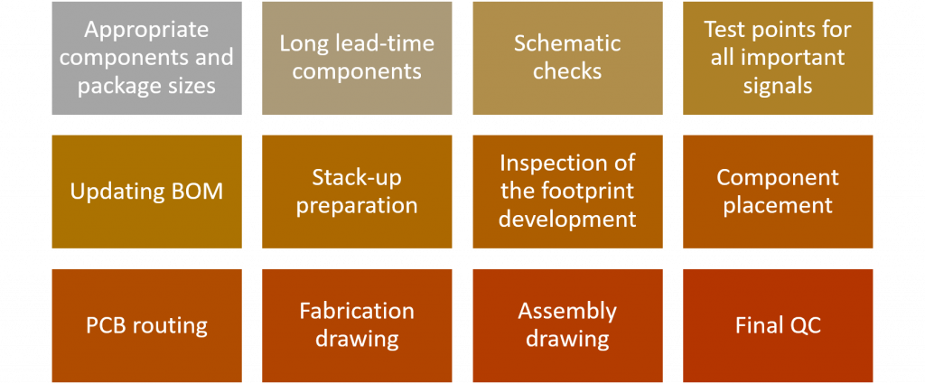
While designing a new PCB, it is necessary to adhere to circuit design basics. If neglected, it will result in a poor board design that will be very difficult to manufacture. Therefore, it is necessary to pay attention to the following concepts:
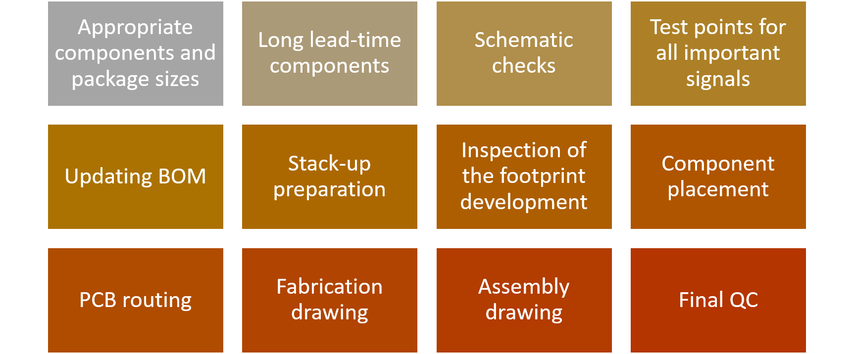
Choose appropriate components and package sizes
As a board designer, you should thoroughly study the BOM and examine the parts that go into the design. When there is sufficient space on the board, you may opt for larger components for resistors and capacitors. It is beneficial to use a 0603 or 0805 size capacitor/resistor instead of a 0402/0201. Select the smaller package version of the component if you have spacing issues. Moreover, choose your appropriate component and package based on the required current, voltage, and frequency.
Smaller components are manufactured by various vendors. It allows designers to choose alternate parts without modifying the schematic or layout, providing a timely solution for components that are not in stock.
Furthermore, it is crucial to decide the appropriate size of the package during the PCB design phase. It is recommended to choose smaller packages only when necessary; otherwise, choose larger packages. Using too many small component packages can create issues during circuit board assembly, which leads to difficulties during cleaning and reworking.
As soon as you determine the ideal package size, you can choose components in the same density category.
Avoid long lead-time components
The unavailability of components can cause considerable delays. So, it is better to check the availability while confirming component spacing. If your component has a long lead-time, order it immediately. It can be beneficial to have alternate components with the same footprint. Assembly vendors can also procure the widely available parts so that every component will be readily available when it is time to assemble the boards.
Schematic checks
A schematic is a well-structured circuit diagram that represents the electrical connections between various electronic components.
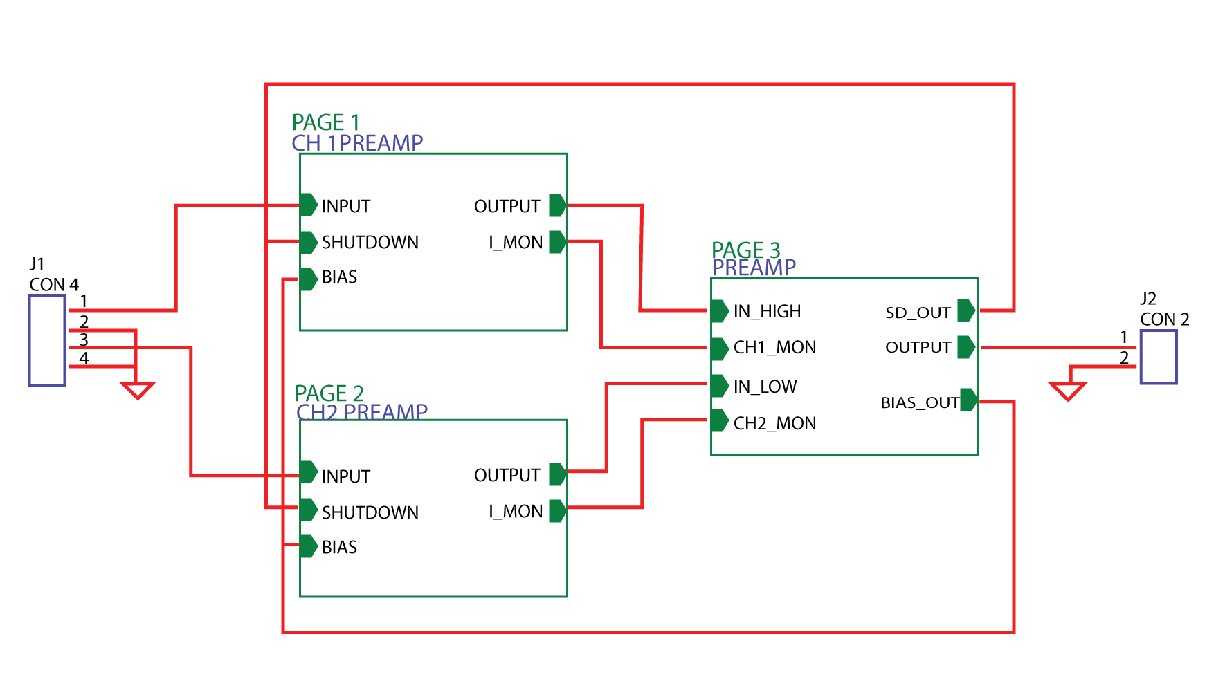
Schematic design basics often get ignored. Make sure you verify the following:
- Verification of pin numbering and labels in component symbols
- A polarity check for all the polarized components
- Overlapping labels and Pins
- Ensuring the base, collector, and emitter pins according to the schematic symbols, datasheet, and footprint package
- Validation of the component value, location, and reference designators
- Descriptions of the schematic symbols
- Off-page connectors
- Checking the inter-sheet reference
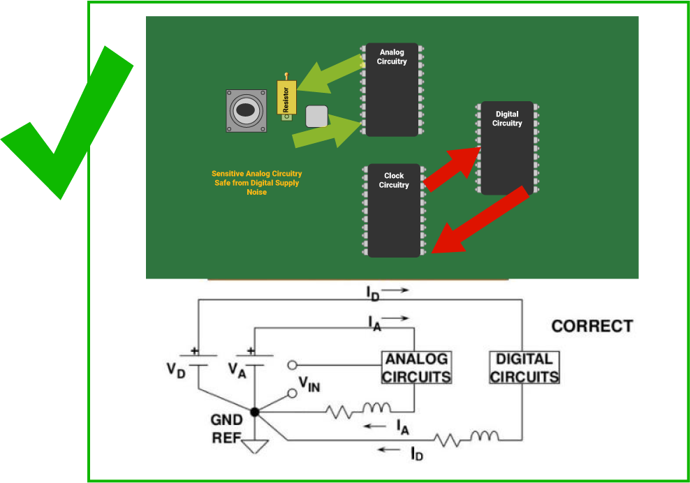
- Decoupling capacitor check for all ICs, ground pin separation according to the signal type (analog, digital, signal, ground)
- Netlist check for design correctness and wrong connections
Read our post on schematic and netlist checks to ensure error-free designs to understand the schematic checks, drafting checks, connectivity checks, and ERC checks.
Add test points to all important signals
Design for testing is required to check the electrical conductivity of the board. It is necessary to add test points for all important signals to facilitate electrical tests (E-test) and in-circuit tests (ICT). Keep an eye on the following:
- Board side: If possible, all test points should be located on the same side of the board to facilitate testing.
- Minimum test point distance: The minimum distance between test points is 0.100 inches. It maximizes test effectiveness.
- Test point distribution: Distributing test points evenly on a circuit board makes testing easier with multiple probes.
- Area for taller components: Designating the area for taller components can streamline the testing.
- Manufacturing tolerances: Make sure to consider manufacturing tolerances while designing a layout to accommodate a space for test points.
Make sure your BOM is up to date while designing
A BOM is a detailed list of all the components required to produce a product. Keep your BOM up to date while designing, and if you make any changes to your design, ensure you have also implemented those changes in your bill of materials. For example, if you change the part number in the schematic, update the BOM as well.

Before you validate your BOM file, ensure that all the active parts are included in it. The parts should be validated with respect to the following fields:
- Serial number
- Part description
- Designators matching the schematic
- Quantity of the parts
- MPN
- VPN
- DNI (do not install) components
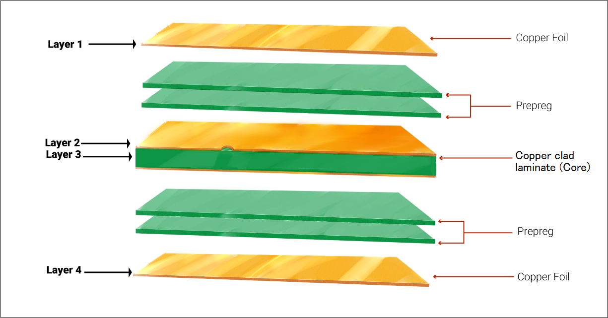
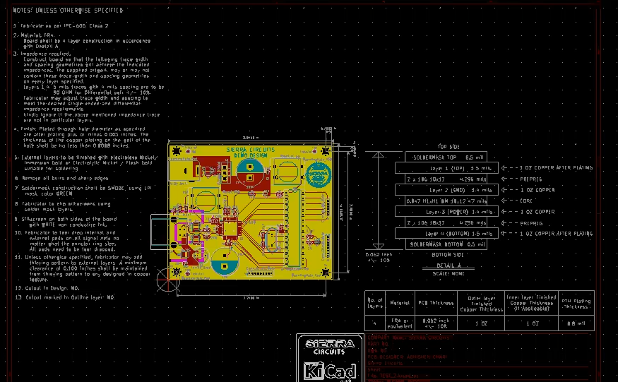
Stack-up preparation in PCB design
Stack-up is an important attribute in the basics of PCB design. It defines the structure of a multilayer circuit board in a sequential manner. Stack-up provides information about the material thickness and copper weights that are vital for circuit board manufacturing. When boards are precisely stacked, electromagnetic emissions and crosstalk are reduced, and the signal integrity is improved.
Know your board’s mechanical constraints, which include board thickness and component height. It is important to know the controlled impedance requirements, including the number of differential pairs, as it will impact the number of layers in your board. The routing density of the circuit board will also impact the number of layers. Choose a PCB material based on the fastest rise time.
Verify the manufacturability of your stack-up using our free Stack-up Planner. The following parameters are necessary for the planner:
- The PCB material (FR4, I-Speed, Rogers, etc.) depends on the frequency requirements and environment.
- Layers including signal and power layers.
- Impedance requirements such as 50Ω single-ended, 90Ω differential, or 100Ω differential
- Copper thickness (½ or 1 or 2 ounces)

Carefully inspect your footprint development
Schematic, complete BOM, and stack-up are the backbone of your circuit board. It is easier to create footprints for some components when they come in standardized packages. In most cases, the footprints of standard packages are available in the software’s library (Altium Designer, Allegro, etc.). Otherwise, you will have to create it based on the datasheet of the component.
Confirm library components match the recommended land pattern provided in the datasheet. After designing your footprint, do a quality check. Mark your component orientation. Footprints must be checked for top and bottom views, pin pitch, and height. Ensuring the accuracy of your footprint as per the land pattern will eliminate PCB manufacturing defects caused by land patterns issues during assembly.
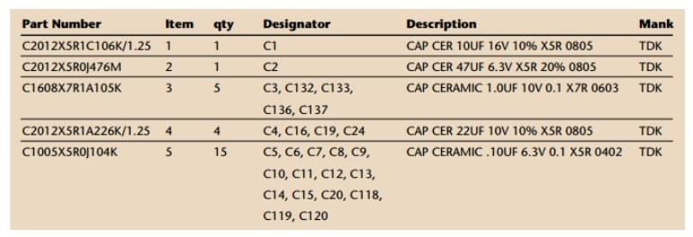
To identify the correct part and its land pattern, it is essential to use the numbering key accurately from the datasheet. An incorrect interpretation of the datasheet will result in the wrong footprint, which may require an entire re-design and re-fabrication of the boards.
The following image shows an example of a numbering key and a variety of footprints.
Placement of components
Once the mechanics of the board have been finalized, next is placing components. The proper component placement on a PCB leads to better performance and signal quality. It begins with placing the parts which are at the specified locations according to the design requirements. These components usually consist of connectors and their associated parts. Following that, the main components such as the CPU, memory, and analog circuits will be placed in their proper positions. The third step involves placing auxiliary components such as crystals, decoupling capacitors, and series resistors.
Also read, How to Place Components in KiCad
Note: Make sure that the mechanical drawing includes the location of mounting holes and parts with critical location and rotation. Check if the drawing has any height restrictions for the top and bottom sides.
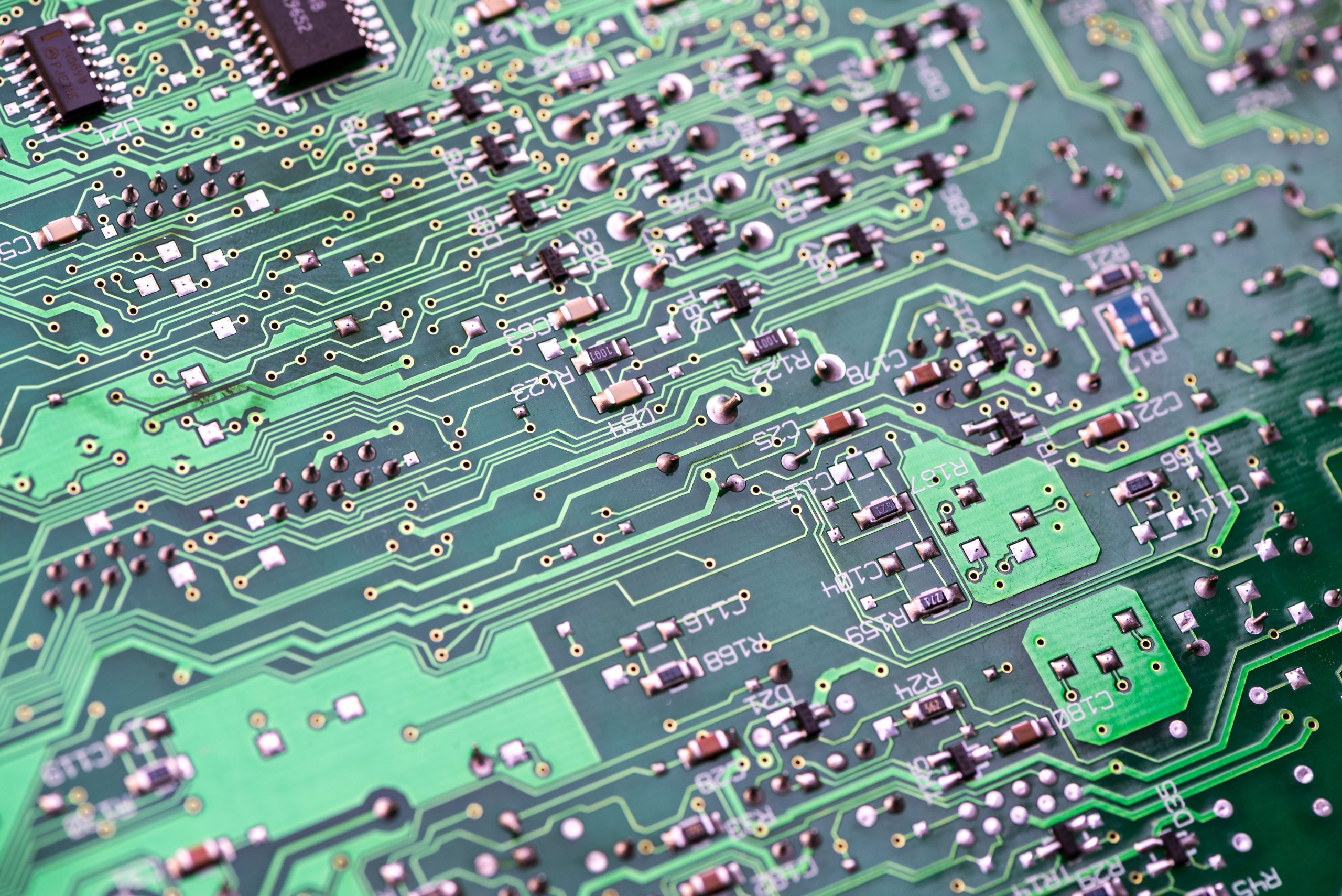
PCB routing
Routing begins with setting design rules for physical spacing and impedance rules. Trace width calculation should be made based on the current requirements of the different circuitry. Assign appropriate rules to the nets accordingly. All controlled impedance traces must have a continuous reference plane layer.
The process of routing involves laying copper traces between the nodes. This conductive path is defined by the placement of traces, vias, and arcs that connect the nodes. After routing, the power/ground plane connections are established.

High-Speed PCB Design Guide
8 Chapters - 115 Pages - 150 Minute ReadWhat's Inside:
- Explanations of signal integrity issues
- Understanding transmission lines and controlled impedance
- Selection process of high-speed PCB materials
- High-speed layout guidelines
Download Now
PCB fabrication drawing
A well-designed fabrication drawing can save time, reduce costs, and eliminate hassle. The fabrication drawing contains information about the fabrication and mechanics of the circuit board. It consists of stack-up information, fabrication notes, IPC standards, and impedance notes.
Fab drawings are sent as PDFs to manufacturers. The fab drawing should contain all the necessary details required to fabricate a board. It should mainly consist of:
- Board dimensions
- Board outline
- Drilling chart
- Stack-up drawing
- Etching tolerance and copper trace
Need help in designing reliable PCBs? Our engineering team can help you with schematics, layout design, and DFM analysis.
You can book a meeting with our experts or call us at +1 (800) 763-7503.

Board assembly drawing
A PCB assembly drawing contains all the information that is required to assemble the board. This drawing can be in a .pdf or .jpg format and can include component outlines, surface mount and through-hole pads, polarity marks, board outline, and titles.
Additionally, assembly drawing consists of a few key points as follows:
- Component outlines: Make sure to display all of the component shapes and their respective reference designators for soldering. It will also include the components that are to be press-fitted or attached with mounting hardware.
- Additional views: Double-sided boards will usually require a view of the front and the backside. Both views can be accommodated on one single sheet if the PCB is small, otherwise, you will need to include additional sheets.
- Manufacturing labels: Identifying manufacturing labels such as barcodes or assembly tags with a pointer and referencing them in the notes.
- Assembly notes: These are a set of instructions containing assembly information, industry standards and specifications, and special feature locations.
Final QC and exporting the correct Gerber files
Once the layout has been completed, the final step is running a set of checks. In this step, DFM (design for manufacturability) is performed to verify the underlying issues associated with the design. These tests will eliminate issues that could have occurred during manufacturing. Using the Sierra Circuits better DFM tool, you can verify the design’s manufacturability. Your design files (in Gerber format) are analyzed, and detailed information about errors in the design rules is displayed.
The final set of deliverables should include all the gerber files, including the fabrication and assembly drawings, drill files, IPC-356, ODB++, and X-Y placement files for assembly. With this information, your fabrication house can perform design for manufacturing (DFM) and design for assembly (DFA) checks on the board.
Let us know in the comment section if you want to learn more related PCB design, manufacturing, and assembly. We will be happy to help you out.

Design for Manufacturing Handbook
11 Chapters - 96 Pages - 90 Minute ReadWhat's Inside:
- Annular rings: avoid drill breakouts
- Vias: optimize your design
- Trace width and space: follow the best practices
- Solder mask and silkscreen: get the must-knows
Download Now


