Contents

On-demand webinar
How Good is My Shield? An Introduction to Transfer Impedance and Shielding Effectiveness
by Karen Burnham
When designing vias for RF PCBs, their impedance should match the desired value in the operating bandwidth. To achieve this, consider the number and placement of stitching vias, pad, and antipad sizes, and the inclusion or removal of non-functional pads.
In this article, you’ll learn the challenges in designing vias for radio frequency circuits and the best layout practices to overcome them.
Highlights:
- Minimize via diameters between 0.2 mm (8 mil) and 0.4 mm (16 mil) or smaller to reduce parasitic inductance.
- Maintain a minimum spacing of λ/20 between stitching vias to minimize impedance mismatches.
- Add a ground return via for channels under 3 GHz.
- Use multiple stitching vias with a properly sized antipad for channels above 5 GHz.
4 types of vias in RF PCBs
Vias are small, conductive pathways that connect different layers of a multilayer PCB. In RF board design, vias are crucial since they transfer high-frequency signals between layers without introducing significant signal degradation.
While they are simple in theory, the design and placement of vias can have a substantial impact on RF performance, particularly at higher frequencies (1 GHz to 30 GHz).
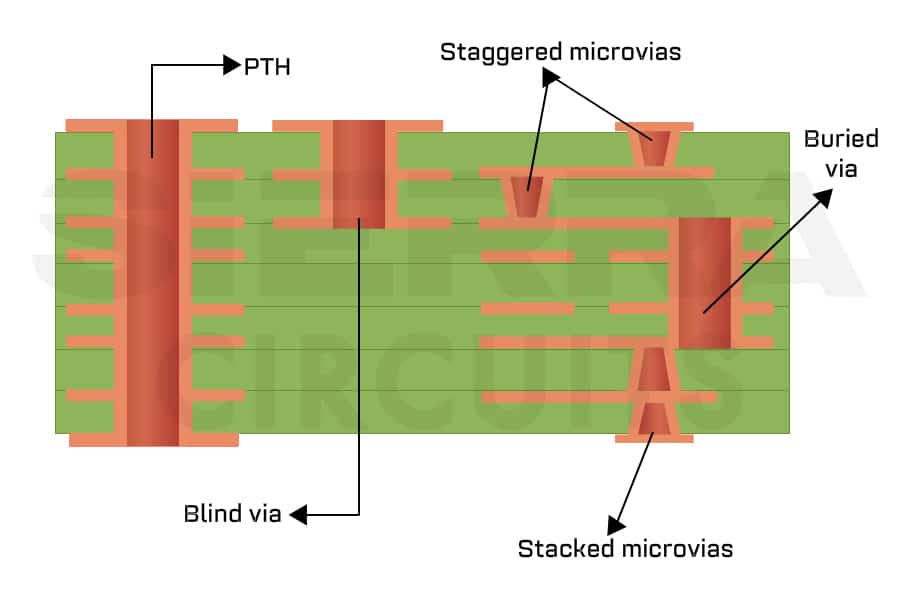
These are the 4 types of vias used in RF PCBs.
| Via Type | RF Application |
|---|---|
| Through-hole vias | Less ideal for high-frequency applications due to their larger parasitic inductance. |
| Blind vias | Valuable in high-frequency RF applications as they reduce signal loss by shortening connections between layers, enhancing signal integrity. |
| Buried vias | Improve space efficiency and RF isolation by keeping connections entirely within the inner layers. |
| Stitching vias | Placed along RF traces to enhance grounding and shielding, helping to control EMI and prevent signal integrity issues. |
For more on vias, see how PCB vias interconnect circuit board layers.
Designing efficient via transitions for radio frequency circuits
Consider these 4 factors when designing vias for RF boards:
- The number of stitching vias used to connect different layers.
- The geometric placement of stitching vias around the primary plated hole.
- Pad and antipad sizes.
- Inclusion or removal of non-functional pads (NFPs)
The primary goal is to maintain consistent impedance and minimize signal reflection.
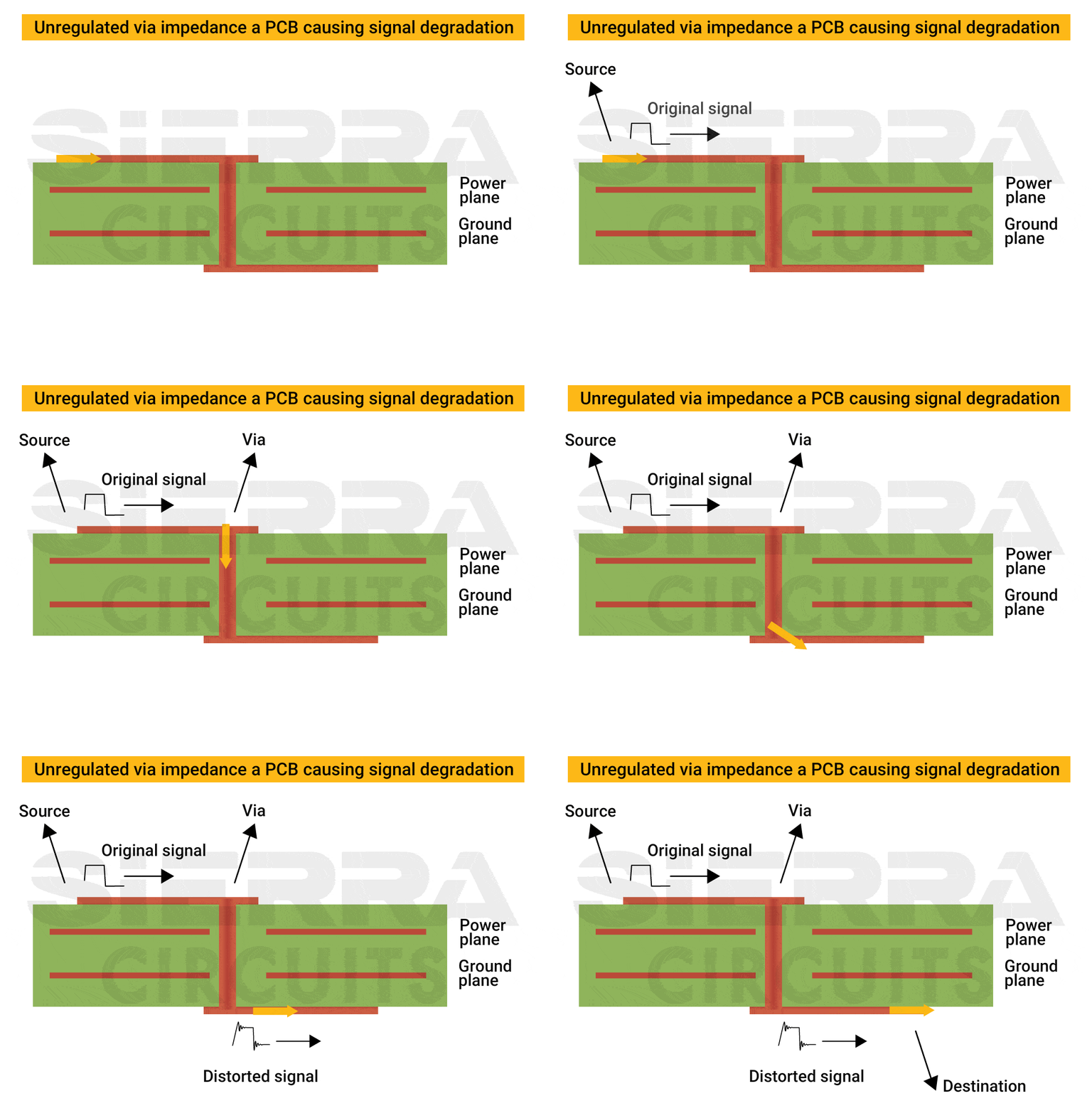
Poorly designed vias can significantly increase insertion loss, limiting the channel’s bandwidth. Thus, careful design of via transitions is essential to avoid signal integrity issues.
7 best practices for designing RF vias
- Design the via to maintain low return loss at the input, especially when dealing with wide bandwidths extending into the GHz range.
- Ensure the presence of vias does not negatively impact the insertion loss. While insertion loss is not usually the focal point for vias, it is still a critical factor.
- Maintain a minimum spacing of λ/10 between the ground vias. For instance, at 2.4 GHz, the clearance should be 6 mm.
- Place ground-connected vias near the PCB edges to reduce RF losses through the laminate. The EMFs are less confined near the edges. However, avoid placing them too close to the edge to prevent mechanical issues.
- For mmWave PCBs, implement a via fence around grounded coplanar waveguides to enhance high-frequency isolation. This technique also suppresses frequencies below a cut-off and prevents mmWave interference with other signals.
- Avoid return or stitching vias for slow-speed signals with rise times higher than 20 ns (e.g., GPIOs, I2C, and control signals) because such signals are less sensitive to impedance discontinuities.
- Prioritize transition methods and the implementation of return paths (e.g., stitching vias) for higher-frequency signals or those with fast rise times to minimize radiation or crosstalk.
RF & Microwave Design Guide
8 Chapters - 44 Pages - 60 Minute ReadWhat's Inside:
- Basics of RF and microwave board design
- Choosing RF materials
- Trace, grounding, via, and stack-up design
- Component selection and placement
- Testing and isolation requirements to avoid interference
Download Now
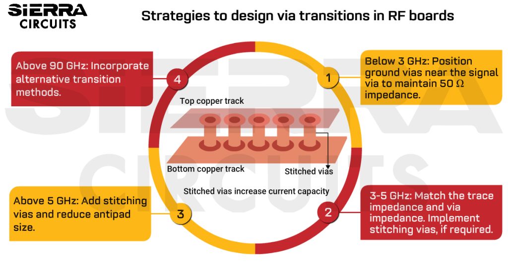
Strategies for designing via transitions in the radio frequency range
Vias may not significantly affect signal integrity at low frequencies (below 3 GHz), as their impedance matches the downstream transmission line. This changes at high and mmWave frequencies, where vias can impact the signal transmission.
To design an effective via transition for high-bandwidth signals, follow these key guidelines:
| Frequency range | Key considerations | Design recommendations |
|---|---|---|
| Below 3 GHz |
|
|
| 3–5 GHz |
|
|
| Above 5 GHz |
|
|
| Above 90 GHz |
|
|
Through-hole via transitions in RF boards
Through-hole via design for RF PCB can support radio signals up to 100 GHz, with consistent impedance up to 50 GHz in digital signals. Achieving higher bandwidths depends largely on the fabrication technology and specific design practices.
4 key considerations for designing plated through-hole vias
When placing a PTH in an mmWave PCB, consider the following factors:
- Uniform impedance: Ensure the via’s impedance aligns with the system’s target impedance (typically 50 Ω) within the signal bandwidth.
- Insertion loss: Verify that the insertion loss remains within acceptable limits throughout the signal bandwidth to avoid performance degradation.
- Propagation delay: If the via is a part of a phase-matched interconnect, the propagation delay across the via must be calculated and factored into the design.
- Eigenmode frequency: The lowest-order eigenmode frequency of the via should be higher than the signal’s wavelength. This ensures continuity and avoids impedance discontinuities as the signal passes through the via.
9 tips for designing through-hole-via transition in microwave and radio boards
- Utilize modern through-hole vias for mmWave frequencies. These through-holes can support high-frequency applications like 77 GHz radar designs. They also demonstrate effectiveness in dense configurations such as 5G mmWave antenna arrays and beamformed MIMO radars.
- Choose smaller drill sizes for through-hole vias to reduce inductance and improve signal quality.
- Design the plated through-hole via to match the input impedance of the interconnect (typically 50 Ω) within the signal bandwidth, ensuring minimal signal reflection.
- Optimize the clearance between stitching vias around through-holes to maintain signal confinement.
- Consult contract manufacturers on advanced fabrication techniques, such as laser drilling, if using through-hole vias in designs operating above 90 GHz, to achieve tighter tolerances and improved bandwidth.
- Ensure insertion loss is kept within acceptable limits by carefully considering the via’s impact on the signal integrity.
- Select RF PCB materials with a lower Dk to shift resonance effects to higher frequencies, reducing their impact on the signal path.
- Consider using blind vias to minimize the risk of signal leakage between layers. Through-hole vias can still be effective, but they require careful placement and must be supported by adequate stitching vias to contain the signal within the intended layers. Apply the following DRC values for stitching vias:
- Default via/pad clearance: 20 mil
- Minimum boundary clearance: 20 mil
- Use reliable via impedance calculators when designing for frequencies above 3 GHz.
Besides the above tips, consider non-through-hole techniques like aperture coupling and stepped blind/buried vias for more accurate layer transitions at GHz frequencies, overcoming the ~90 GHz limit. They offer improved control over signal flow. Always minimize the through-hole via count in high-speed traces to limit parasitic inductance and capacitance. Read drills and through-hole plating to discover the differences between mechanical drilling and laser drilling in printed circuit board manufacturing.
4 challenges in designing vias for RF PCBs
Improperly designed vias can act as unwanted inductors or capacitors or cause transmission line discontinuities. This leads to impedance mismatches, parasitic inductance, and excessive crosstalk.
1. Parasitic effects in vias cause RF signal distortion
At RF frequencies, even a small discontinuity in a signal line, such as vias, can disrupt signal transmission. This can lead to reflections, losses, or distortions.
Vias inherently introduce parasitic capacitance and inductance, which can negatively impact the RF signal transmission. This undesired capacitance occurs when plated holes create unintended capacitive coupling between the signal and ground layers. Parasitic inductance arises from the loop created by the via structure.
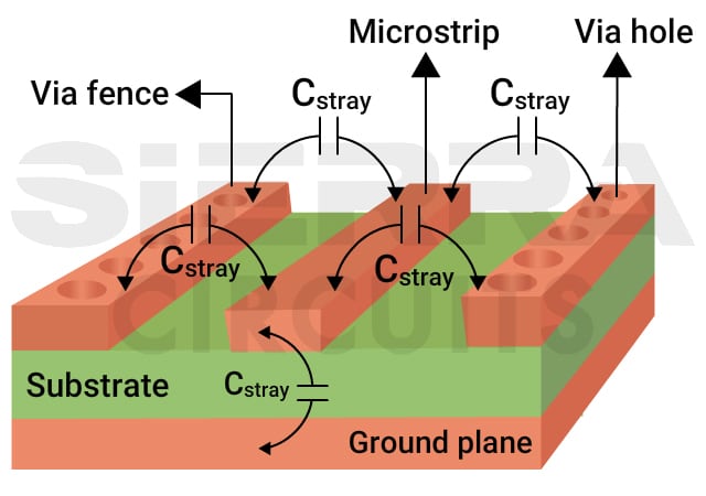
To minimize these parasitic effects, consider the guidelines given below.
17 via design strategies to ensure signal integrity
- Limit the use of vias when routing radio-frequency traces. When unavoidable, place ground vias close to signal vias to enhance signal integrity.
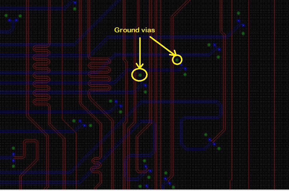
Ground vias (green dots) placed near the signal vias to enhance signal integrity. - Do not use larger vias, as incorporating them does reduce the inductance, but it is not efficient. Implementing large vias is not practical in compact or HDI designs.
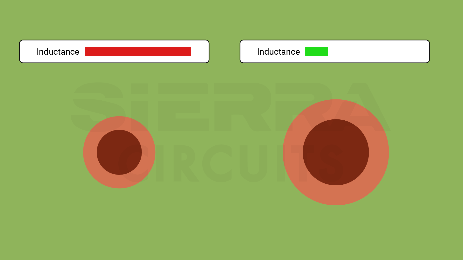
Larger vias do not significantly reduce inductance.
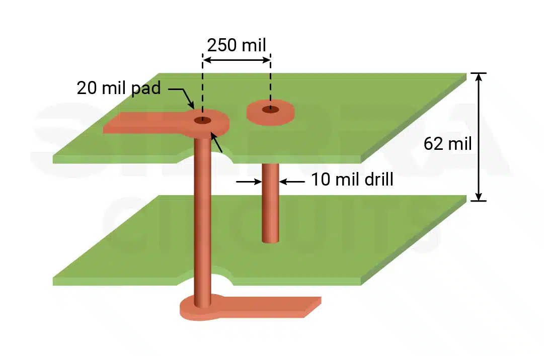
As described by Rick Hartley, consider two vias with 10 mil drill and 20 mil pad in a 62 mil-thick board that are 250 mil apart. The approximate inductance will be 2.5 nH. If you double the via size, the inductance will drop to 2 nH. That’s only a 20% drop in inductance, not impactful enough to justify larger vias.
- Keep the vias close to each other.
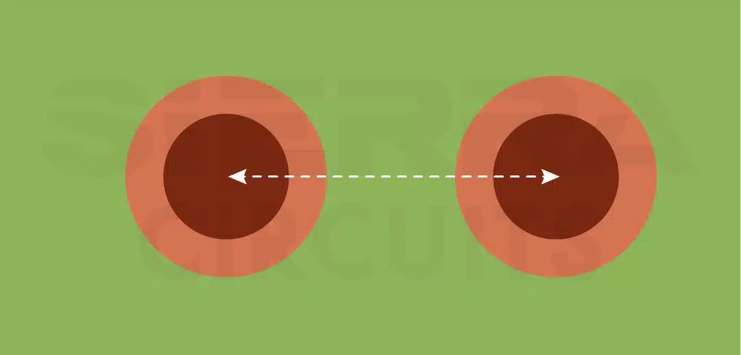
Position vias closer to each other to minimize inductance.
As Rick Hartley rightly quoted,
“Inductance is a proximity effect more than a size effect.”
Place the vias as close as possible to minimize the inductance.
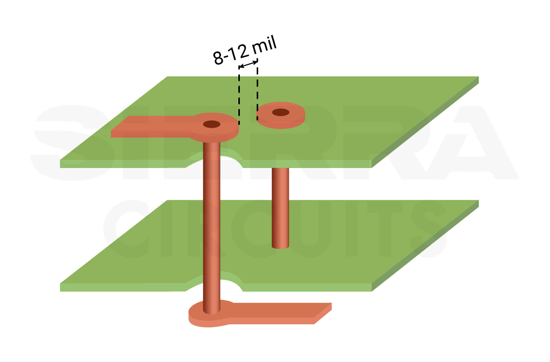
Consider two vias with 10 mil drill and 20 mil pad in a 62-mil-thick board. But now they are apart by 8-12 mil. The approximate inductance will drop to 1 nH. That’s a 50% drop.
- Reduce via diameters to 8–16 mils to improve routing density, and enable tighter placement, an approach that more effectively reduces inductance by minimizing loop area than simply enlarging via size.
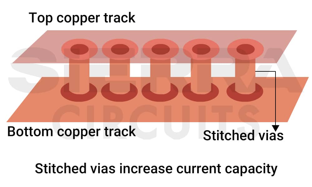
- Add multiple parallel vias to increase the overall cross-sectional area for current flow, ensuring even current distribution and effectively reducing parasitic inductance.
- Use dedicated vias for each RF component pin.
- Include sufficient ground vias for the central pad of QFN packages to reduce parasitic inductance and ensure the same ground level between the IC and the rest of the board.
- Place at least two vias at each point where a PCB transmission line crosses from one layer to another to minimize the resulting inductance variation. A via pair can reduce inductance variation by 50%, provided the diameter of the trace is compatible with the trace width.
- Place ground vias on RF traces and near radio frequency components to provide efficient return paths and minimize coupling.
- Do not place multiple power vias next to each other, as this increases the inductance due to the solenoid effect, where closely spaced same-type vias create larger loop areas. Instead, arrange them in alternating power-ground pairs to minimize the loop area, significantly reducing inductance.
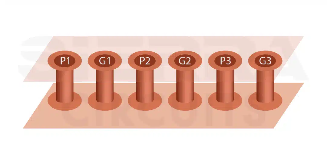
Place vias in alternating power-ground pairs to reduce the loop area. - Implement via stitching wherever applicable to create shorter ground return paths for the current.
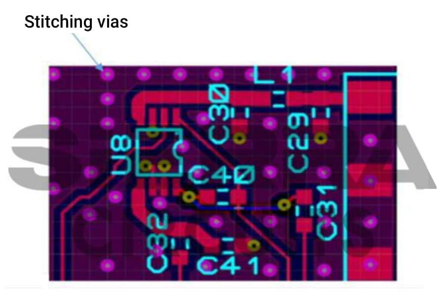
Via stitching on a circuit board layout. - Always match via impedance with the impedance of the RF circuit by precisely calculating via dimensions (diameter, pad size, and distance to the ground plane). Accurate via impedance calculations ensure signal integrity.
- For differential signals, match via diameters to ensure consistent impedance and minimize skew. Adjust the vias for single-ended signals independently to meet their specific impedance requirements.
- Coordinate with your PCB manufacturer to verify feasible via sizes based on their equipment precision and process capabilities, avoiding expensive redesigns.
- Employ back drilling to remove via stubs.

Back drilling to remove via stub.
- Fill vias with conductive materials such as copper or epoxy. This approach improves mechanical strength, eliminates air gaps, and enhances thermal and electrical conductivity, thereby minimizing signal losses in high-frequency applications.
- Implement via-in-pad to eliminate excess stub lengths. This approach reduces radiation and signal reflections at high frequencies.
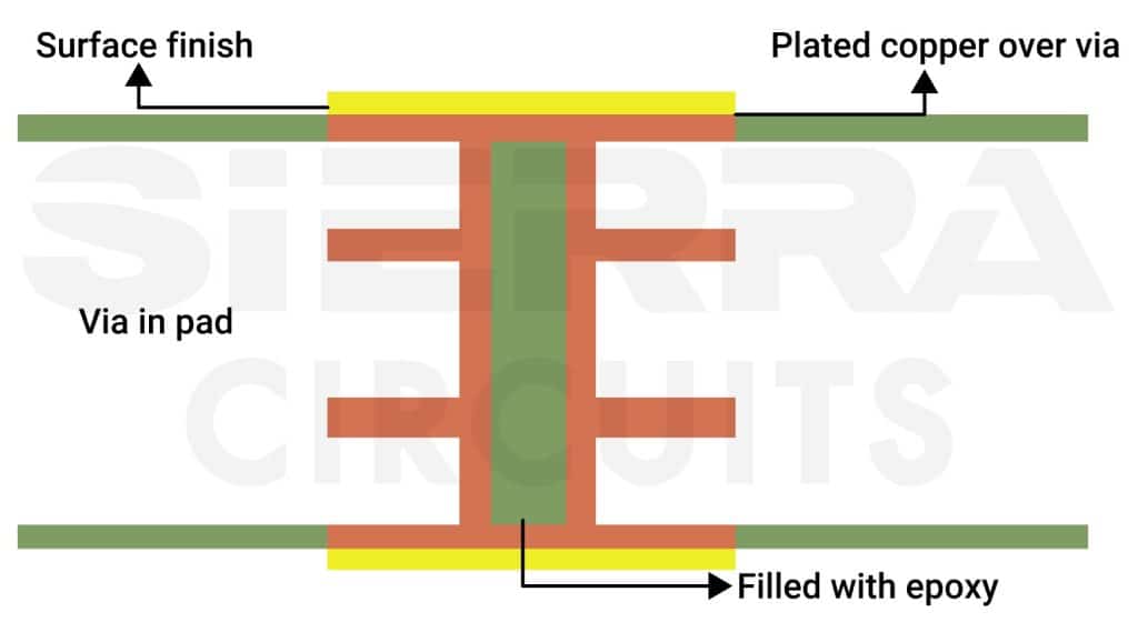
At Sierra Circuits, we ensure enhanced precision in via-in-pad and back-drilling processes by utilizing our mechanical vision drilling and routing machine. This advanced technology minimizes errors by automatically realigning the board during multiple drill programs.
See RF and microwave PCB capabilities to learn more.
2. Insufficient via spacing introduces impedance mismatches
When vias are placed closely together, they can interact with each other, causing increased impedance and unwanted coupling between signals. Tight via spacing also makes isolating sensitive RF signals from other traces harder, leading to crosstalk in high-speed PCBs.
6 via sizing and spacing considerations
- Consider the circuit’s current requirements, mechanical stress, and resilience to thermal expansion when selecting the optimal via depth. As via depth increases, impedance rises due to increased capacitance between the planes. A shallower via has lower capacitance, and it is more susceptible to cracking during reflow soldering.
- Use a lower aspect ratio to optimize signal performance, as higher aspect ratios can increase inductance and degrade signal quality. In RF boards, the typical aspect ratio ranges from 0.8 to 1.2.
-
Space vias farther apart to lower their impedance, as fewer vias in a given area lead to reduced impedance compared to densely packed vias.
- Employ flagship tools such as ADS, Pathwave, Ansys, and HFSS to model and simulate wave propagation in microwave and RF designs.
- If possible, utilize the maximum number of vias to transition from the ground fills on the top layer to the inner ground layers, ensuring effective grounding and minimizing impedance issues.
- Select the via stitching gap between λ/20 and λ/10, depending on the specific value of λ. If λ is too small to accommodate λ/20, opt for λ/10 instead. The optimal spacing should ultimately be determined through calculations and tailored to the specific application requirements.
| Frequency (GHz) | Wavelength (cm) | Spacing between stitching vias: 1/20th wavelength (mm) |
|---|---|---|
| 2.5 | 12 | 6 |
| 3.0 | 10 | 5 |
| 4.0 | 7.5 | 3.75 |
| 5.0 | 6 | 3 |
- Adjust the antipad dimensions to control the capacitance associated with a via and directly control its impedance. Antipads are the gaps between the via plating and nearby copper structures.
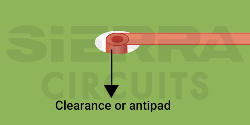
In high-speed and RF PCB designs, via transitions must pass through at least one plane layer, making it essential to size the antipad correctly in the plane layer to determine impedance effectively.
Use the following formulas to calculate via inductance and capacitance theoretically:
Inductance of via:

Capacitance of via:

where,
L = Length of the via
b = Clearance diameter
a = Via diameter
Although via drill size significantly impacts the impedance, keep the via drill size constant and adjust the antipad dimensions instead, as this change does not affect the cost.
Using the equations above, we can create a table showing how via impedance varies with different antipad dimensions. The theoretical values indicate that an antipad radius of 0.6 mm or 0.65 mm (corresponding to diameters of 1.2 mm and 1.3 mm) offers optimal return loss.
| Antipad radius (mm) | Capacitance (fF) | Inductance (fH) | Impedance Z (Ω) |
|---|---|---|---|
| 0.4 | 56.19565383 | 75553.04268 | 36.66694 |
| 0.45 | 44.93494464 | 75553.04268 | 41.00472 |
| 0.5 | 38.10469405 | 75553.04268 | 44.52836 |
| 0.55 | 33.49852836 | 75553.04268 | 47.4912 |
| 0.6 | 30.16916553 | 75553.04268 | 50.04311 |
| 0.65 | 27.64190988 | 75553.04268 | 52.28077 |
| 0.7 | 25.65235349 | 75553.04268 | 54.27032 |
| 0.8 | 22.70742627 | 75553.04268 | 57.68223 |
| 1 | 19.05234703 | 75553.04268 | 62.97262 |
Consider varying antipad dimensions for vias on critical traces at higher frequencies. For simple designs with return paths directly under the trace, you can calculate via impedance manually. However, for complex PCBs, it’s better to use a 3D solver to account for all possible return paths and achieve more accurate results.
For more high-speed design rules, download our design guide.

High-Speed PCB Design Guide
8 Chapters - 115 Pages - 150 Minute ReadWhat's Inside:
- Explanations of signal integrity issues
- Understanding transmission lines and controlled impedance
- Selection process of high-speed PCB materials
- High-speed layout guidelines
Download Now
3. Inadequate ground vias increase EMI issues
Ground vias are critical for RF PCBs in reducing noise and maintaining signal integrity. By strategically placing them near signal vias, you can create an efficient signal return path for high-frequency currents, reducing EMI in circuit boards.
Placing a ground via far from a shunt component alters the component’s impedance at the trace, causing impedance mismatch. We have listed a few radio circuit board design guidelines to ensure reliable vias.
10 grounding strategies to mitigate interference
- Form ground shielding around the RF section using vias whenever possible.
- Incorporate numerous ground vias throughout the RF section, maintaining a maximum spacing of λ/20 between ground fills on the top and inner ground layers.
- Distribute vias evenly along both sides of the transmission line to isolate noise from adjacent traces or ground layers.
- Assign dedicated vias for each RF IC pin, ensuring no via is shared between multiple pins or pads.
- Avoid daisy-chaining ground connections, which can increase loop inductance and degrade performance.
- Place ground vias directly next to pins or pads on the top layer and add additional vias wherever feasible. Using multiple ground vias in parallel reduces the total parasitic inductance of the via network compared to a single via.
- Employ at least two grounding vias for each shunt-connected component, such as power-supply decoupling capacitors, to minimize the impact of via parasitic inductance. Create via ground islands for groups of shunt-connected components to further enhance grounding efficiency.
- Maintain a solid ground plane on the component layer (top or bottom of the PCB) beneath the IC to support DC and RF return currents. This ground paddle also serves as a thermal heatsink. Preferably plated and filled with thermally conductive paste, the paddle should include the maximum number of through-vias permitted by design rules.
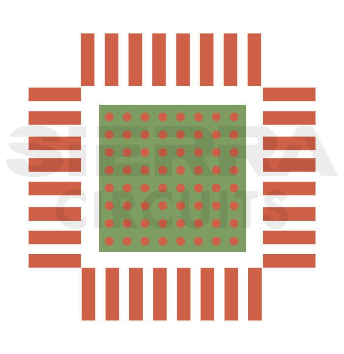
A ground paddle with vias under an IC. - Apply via fencing, a widely used and cost-effective technique for spatial isolation. It shields microstrip and stripline transmission lines, creates fencing around circuit board edges, and separates distinct functional units on the same board. This method, commonly used in modern circuit boards to isolate BLE and Wi-Fi units, mitigates parasitic coupling between closely spaced traces by forming an effective via barrier.
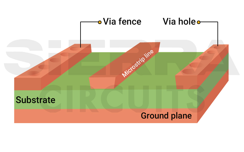
Via fencing in microstrip lines. - Install via fences on both substrates above and below the RF trace in stripline transmission lines, ensuring these vias are grounded through the respective top and bottom ground planes.
- Connect via fencing on the top layer of microstrip lines with a metal track, as the top side does not have a ground plane.
- Utilize via stitching in microstrip and stripline designs to improve isolation between signal and ground planes. Via stitching helps establish continuous ground connections across different PCB layers, reducing ground loop areas, minimizing signal degradation, and controlling impedance.
Need help in planning via structures for your RF layout? Check out our PCB design support.
4. Poor via design leads to overheating of components
Thermal dissipation is a key concern in RF PCB designs. Vias not only serve as electrical pathways but also affect heat transfer. Poorly designed vias can hinder thermal management and cause overheating of components, potentially damaging the PCB.
6 via design tips for thermal management in RF boards
- Integrate thermal vias into the PCB stack-up to enhance heat transfer and distribution.
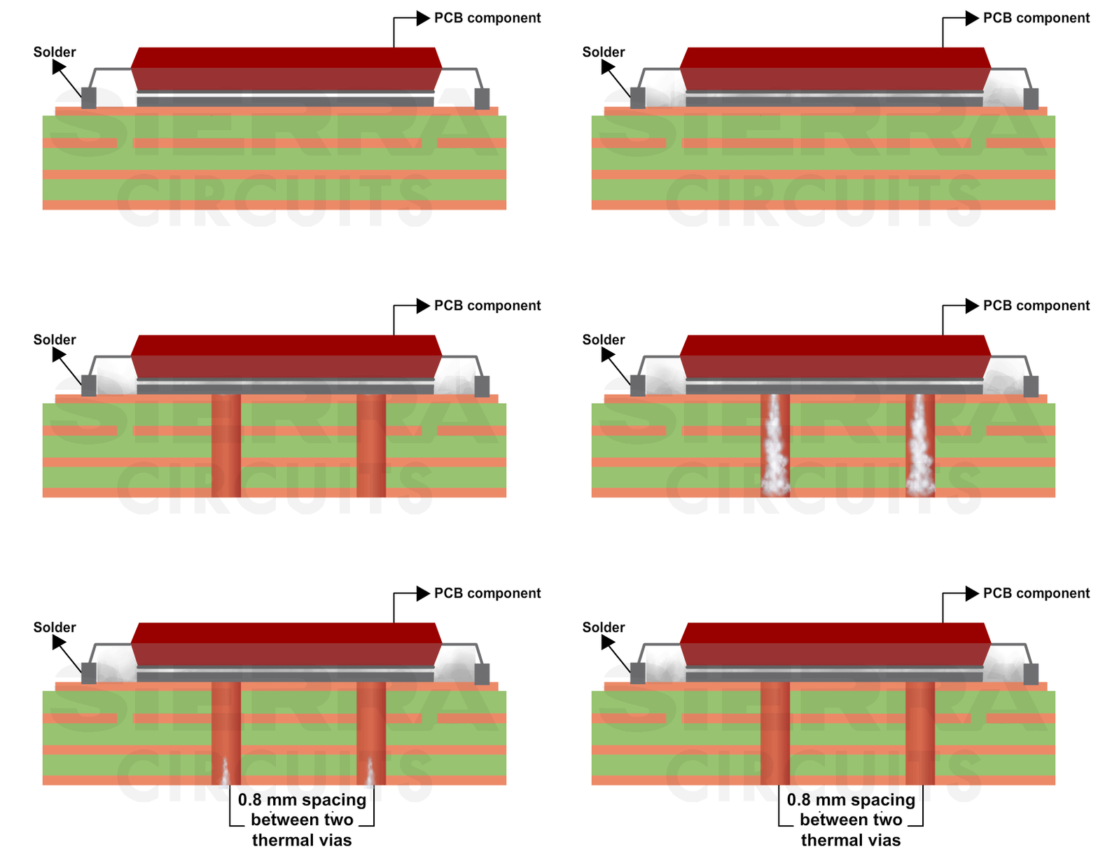
Position thermal vias close to heat-generating components to create an efficient thermal path. - Ensure the vias connecting the ground pours include proper thermal relief patterns to enable effective soldering and heat dissipation.
- Incorporate a greater number of smaller PTHs within a ground pad to create a more efficient thermal path than fewer larger PTHs.
- Use a through-hole wall thickness of 0.1 mm for applications where heat transfer is critical. For standard applications, the standard 0.025 mm thickness is sufficient.
- Use proprietary via plugging paste to fill the PTHs beneath components and plate over the top surface to create a continuous ground pad. Applying electrically and thermally conductive paste, such as silver (Ag)-loaded epoxy, to fill the PTHs can improve thermal conductivity compared to non-conductive fillers. However, note that the overall thermal conductivity of these pastes typically ranges from 4 to 30 W/mK, which is relatively low and not worth the added cost.
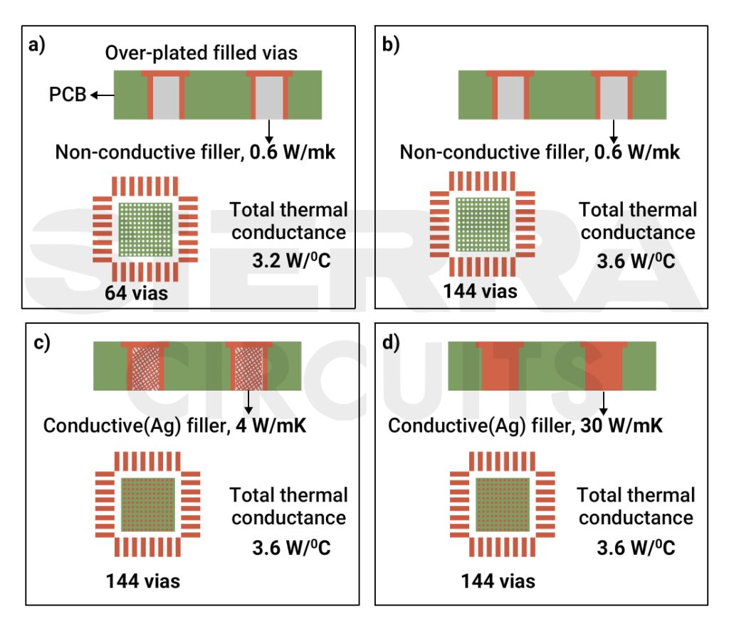
Silver epoxy conductive filling offers slightly better thermal conductance. However, the expense is not worth it. - Increase the plated wall thickness of PTHs from the standard 25 µm to 100 µm to enhance thermal conductivity.
- Integrate copper coins into the circuit, typically stepping them to ensure efficient and even heat distribution.
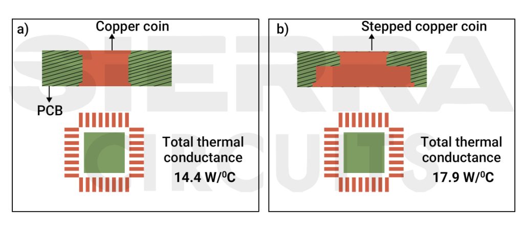
Copper coins in RF PCBs improve the thermal conductivity of your board.
- Transfer heat from components to the core using thermal vias or by direct contact via cavities within the circuit where components are mounted. Thermal vias with blind holes having diameters <0.2 mm and depths <0.3 mm can be filled with copper using a blind hole plating process.
To learn about the hurdles in microwave board design, see microwave PCB design challenges and how to overcome them.
Key takeaways
- Calculate via dimensions precisely (diameter, pad size, antipad) to maintain controlled impedance.
- Add stitching vias near signal vias to ensure effective grounding and minimize EMI.
- Utilize back-drilling or via-in-pad designs to reduce via stubs and mitigate high-frequency signal reflection.
- Minimize parasitic inductance and capacitance by optimizing via diameter and spacing.
- Avoid routing RF traces through vias unless unavoidable; use nearby ground vias to improve signal clarity.
- Place ground vias strategically near signal vias for reliable current return paths and reduced noise.
- Implement via fencing or stitching to enhance RF isolation and minimize crosstalk.
- Apply ground planes beneath ICs with multiple through-vias to support both thermal dissipation and RF performance.
- Use thermal vias to dissipate heat efficiently, especially under high-power components.
- Fill vias with conductive materials like copper or epoxy for improved heat transfer and mechanical strength.
- Increase plated wall thickness for through-hole vias in thermally demanding applications.
- Match via impedance to the system’s target value, ensuring minimal insertion loss and phase mismatches.
- Reduce via spacing to less than λ/20 for frequencies above 3 GHz to minimize coupling and impedance mismatches.
- Focus on mmWave PCB strategies, such as via fences and advanced fabrication techniques, for designs operating above 90 GHz.
- Explore non-through-hole alternatives like blind or buried vias for frequencies higher than GHz.
Via design for RF PCB is a critical factor in achieving reliable performance, particularly as operating frequencies continue to increase. By carefully considering factors such as parasitic effects, controlled impedance, and ground via placement, designers can minimize signal loss and improve overall performance.
Need help designing a microwave circuit board? Post your questions on our PCB forum, SierraConnect. Our design experts will resolve them.
About Pooja Mitra : Pooja Mitra is an electronics and communication engineer. With an experience of over three years in the PCB industry, she creates industry-focused articles that help electrical and PCB layout engineers.


