


Contents

On-demand webinar
How Good is My Shield? An Introduction to Transfer Impedance and Shielding Effectiveness
by Karen Burnham
Implementing decoupling schemes, efficient grounding, circuit safety measures, and capturing a schematic diagram are a few of the best electronic design practices. In this article, we will discuss the best circuit design practices that can build a well-planned board.
Highlights:
- A well-designed circuit board is essential for creating reliable and high-performing electronic devices.
- When designing your circuit, be mindful of the manufacturing process. Consider aspects like component size and placement, trace routing, and the usage of vias.
- Using a standard schematic format can make it easier for others to understand and troubleshoot your design.
- Document your design thoroughly, including creating schematics, layout drawings, and bills of materials for future troubleshooting and maintenance.
- Test your design thoroughly, including building a prototype and testing it under various conditions using simulation software.
Let’s dive right into it with block diagrams.
1. Define specifications and build block diagrams
Your first step in designing an electronic circuit is to develop a detailed requirements specification that covers all aspects of circuit design including:
- Input and output signals
- Voltage/current/power requirements
- Operating temperature and frequency ranges
- Radiation shielding techniques
- Board size
- Component spacing and mounting details
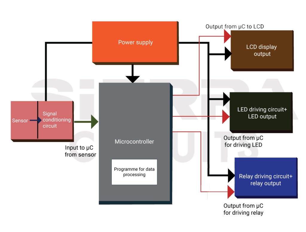
All this should be done keeping in mind the available budget. The next step is to build block diagrams that provide an overview of the circuit functioning and component groupings. Block diagrams are crucial for successful electronic circuit design and act as a reference material for future circuit analysis.
They also allow for a divide-and-conquer strategy where the diagram is broken down into different functional sections, each performing a specific task that can be implemented and tested in isolation. Knowledge and understanding of the operation of each of these blocks are necessary. Some blocks may have signal conditioning circuits so that the output can be read easily by the data acquisition system.
For example, output from an LDR (light-dependent resistor) sensor needs to be converted to a voltage range that can be easily read by the microcontroller ADC. Circuits in these blocks could also be replicated in other designs requiring similar functions, promoting design reuse. To learn more about design reuse, see auto grouping of repetitive PCB design blocks.
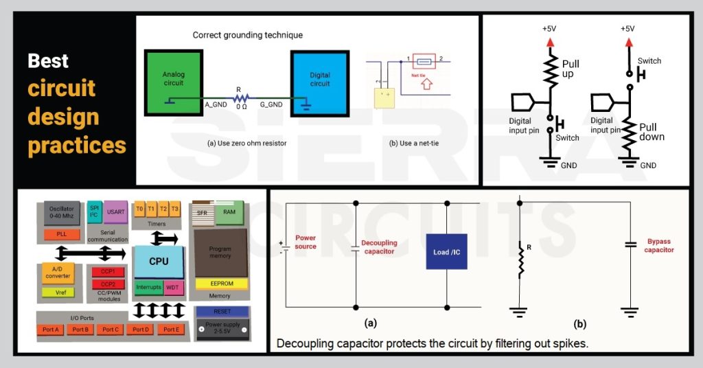
2. Employ pull-up, pull-down, and zero resistors
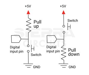
Digital ICs work with certain logic levels to determine whether the input is interpreted as 0 or 1. For a VCC of 5V, voltage levels from 5V to 2.8V are considered logic 1, and 0 to 0.8 as logic 0. The voltage range between 0.9 and 2.7V will be an indeterminate region, and the chip will interpret it either as a 0 or as a 1, causing the IC to behave incorrectly. This is called the floating state.
To prevent this, pull-up or pull-down resistors are used while designing electronic circuits that use digital ICs, microcontrollers, and switches. Pull-up resistors are used to fix the voltage close to VCC, and pull-down resistors to pull the voltage close to the GND point. Modern microcontrollers are now equipped with internal pull-up and pull-down resistors that can be activated using code. Please check the datasheet and decide accordingly if these resistors need to be used or eliminated.
What are the benefits of using zero-ohm resistors?
Zero-ohm resistors can be used to modify the circuit even after its construction. These resistors are used as a bridge to route tracks optimally on a board.
As a circuit board designer, you can make PCBs with multiple configurations and functionalities. Most often, these configurations interfere with each other and cannot all coexist in a circuit. Hence, based on requirements, different sections of the PCB can be disabled or enabled easily by unsoldering or adding zero resistors accordingly.
You can divide the circuit into multiple sections by using zero resistors. This is helpful in isolating faulty segments that need troubleshooting. For example, it is easy to find noisy blocks and traces that cause crosstalk without having to cut up the circuit.
A section of the circuit might need a series resistance whose value needs adjustment and isn’t fixed yet. Until the value is finalized, zero resistors can be used temporarily. Zero resistance pads also serve as a test or debug point to measure various parameters like voltage, current, etc.
SMD zero resistors facilitate continuous connection and are used to replace jumpers. This will allow for an efficient single-layer board design instead of a double-layer board. They are much cheaper than DIP switches or Berg jumpers. Zero-ohm resistors are also used as circuit breakers during supply overload, preventing circuit damage.
Due to the reasons mentioned above, using zero resistances during prototyping in the initial design phase is a good practice.
In RF circuits, zero resistors can be inserted into an RF feed in series with the antenna trace. As the antenna is tuned, it can be replaced with other values. It is also used as a matching element in some RF applications.
Wired resistances, i.e., traces connected by zero ohms, work well for digital circuits. However, high-speed circuits will not work due to the high value of their parasitic inductance. The maximum permissible current, the enclosure type, the footprint on the PCB, the parasitic inductance, and the capacitance of the resistor are different parameters to be looked at while choosing a zero resistor.
3. Utilize microcontrollers and mixed-signal circuits to increase performance efficiency
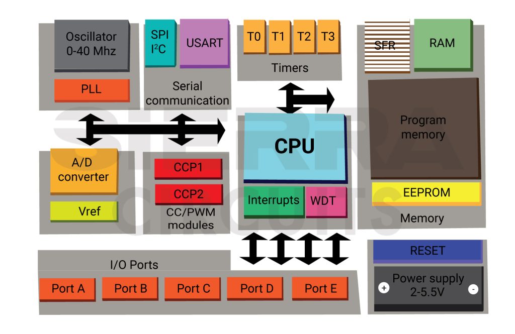
Mixed-signal circuits are hybrid circuits that combine both analog and digital circuitry in a semiconductor die. This is also referred to as system-in-package. Depending on the design requirements, you should make use of modern low-cost microcontrollers as they have several built-in features. The most commonly used microcontroller peripherals are timers, pulse-width modulators (PWM), analog-to-digital converters (ADC), digital-to-analog converters (DAC), and serial/SPI/ I2C communication interfaces.
They can be easily programmed to function according to the requirements. This will avoid overkilling your circuit with too many discrete components to perform the same task. Integrating appropriate digital ICs and analog circuit sections with a microcontroller will increase the performance efficiency of the circuit while reducing its size and cost. A block diagram of a microcontroller is shown below.
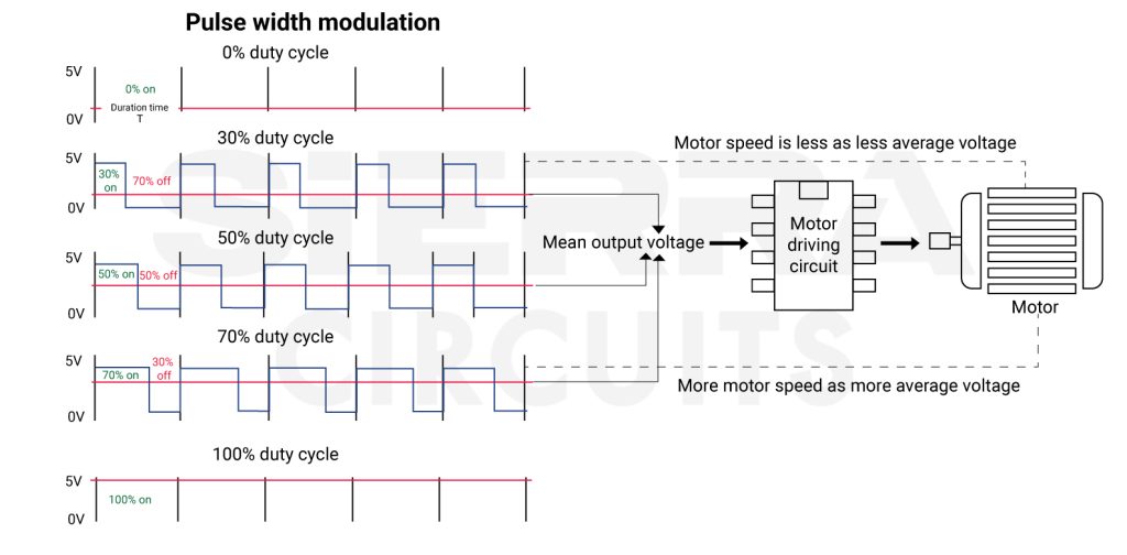
4. Reduce power consumption using PWM signals
Building a circuit that saves energy is important, especially for those that are operated with batteries. PWM is a type of modulation where the pulse width of a signal is modified based on the duty cycle.
A PWM signal with a 75% duty cycle will stay ON for 75% and OFF for 25% of the total time period, thus reducing the mean output power consumption. These signals can be generated using a reliable microcontroller or NE555 IC. It can be employed to save energy in simple LED and motor driving circuits. PWM waveforms are also used in power converter(s) topology to design highly efficient, lighter, and inexpensive switched-mode power supply designs.
5. Implement safety measures for ESD, reverse polarity, transients, and over-voltages
Protecting circuit connections from ESD is essential if the product is used in harsh conditions. Metal-oxide varistors, TVS (transient voltage suppressor) diode arrays, clamping diodes, and GDTs (gas discharge tubes) can be used to safeguard from ESD. Between the diodes and ICs, a resistance of a few tens of ohms can be placed to dissipate a voltage surge. This should be especially implemented at communication interface connections, user button contacts, and other sensitive input/output connections.
Reverse polarity protection in a circuit can be provided by different types of diodes or by using FET circuits. Diodes usage is mostly suitable for low-power applications.
For overvoltage protection, voltage limiters can be used in conjunction with electronic fuse chips and thermistors. Modern ICs now come with built-in protection circuits. Examples of voltage limiters are varistors, TVS diodes, and diode circuits (clipping and clamping). Fusechips can be either hotswap circuit ICs or power controllers.
Protection diodes should also be used when relays are being driven by semiconductors. If the power to the relay coil is shut off suddenly, the coil will generate a voltage spike that can damage the rest of the circuit. A flyback diode acts as a snubbing circuit, providing a discharge path for the coil in order to protect your circuit. Using microcontrollers for a protective shutdown circuitry should be avoided as they might freeze.
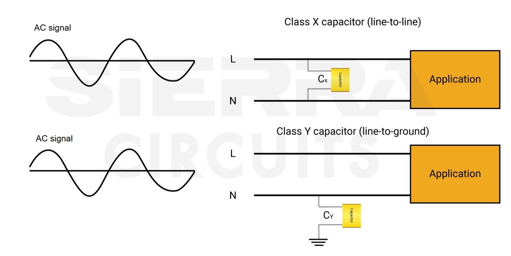
High-voltage capacitors used in the circuit must be provided with proper discharge paths. If devices in a circuit are deriving power from a network, a good understanding of class X/class Y safety capacitors and their proper placement is essential. These capacitors are used to filter AC signals and reduce EMI, as shown in the figure below. They also mitigate the adverse effects of voltage transients and overvoltage surges.
Class X capacitors are typically placed between the line and neutral of the AC supply to reduce EMI/RFI due to differential mode noise. Class Y capacitors are ideally placed between the AC supply and ground to minimize common-mode noise. There are varying standards and classifications for safety capacitors that indicate their threshold capacities. You should choose the right capacitors based on the design needs.
You must choose optimal combinations of the above-mentioned protection schemes by considering error probabilities, reliability requirements, and PCB space and cost constraints.
When you’re working with high voltages, proper PCB grounding techniques such as galvanic isolation must be provided to avoid electric shocks. This prevents potentially damaging currents from passing through the operator’s body or to other parts of the circuit.
Galvanic isolation is also used when two sections of a circuit have different ground potentials and a signal needs to be transferred between them. It prevents the flow of unwanted AC and DC currents between the two parts. Isolation breaks these ground loops that cause signal inaccuracies between the two systems, maintaining communication integrity.
A popular option is to use transformers for stepping up/down voltages, along with using electric fuses. The exchange of information between isolated sections is provided by using optoisolators, hall sensors, capacitors, or relays.

Signal Integrity eBook
6 Chapters - 53 Pages - 60 Minute ReadWhat's Inside:
- Impedance discontinuities
- Crosstalk
- Reflections, ringing, overshoot and undershoot
- Via stubs
Download Now
6. Select the components based on the life cycle
The components need to be selected based on the design requirements and adequate margins. Many different packages are available on the market – through-hole, surface mount, panel mount, and chassis mount to take advantage of various requirements.
Consider these tips while choosing components for your electronic circuit design:
- Read component datasheets extensively and incorporate them in the design based on the reference circuits or calculations they specify.
- Ensure that you use parts that won’t become obsolete and will remain available for the next 5-7 years at least.
- Derate parts to avoid operating them near their limits, which could eventually lead to failure.
- Choose parts that have 1.5 -2 times more ratings than the actual required values. For example, the resistor wattage rating should be such that only 50% of the rated wattage should be dissipated in it. Similarly, transistors, diodes, ICs, input sources, connectors, etc., should be selected keeping similar overrating in mind.
- Keep a spreadsheet with power dissipation calculations for each part along with its values, types, and packages to prepare a clean bill of materials.
- Use standard component values as much as possible to keep the circuit costs down. It is also good to avoid parts that have a large lead time.

7. Effectively capture the schematic and verify using EDA tools
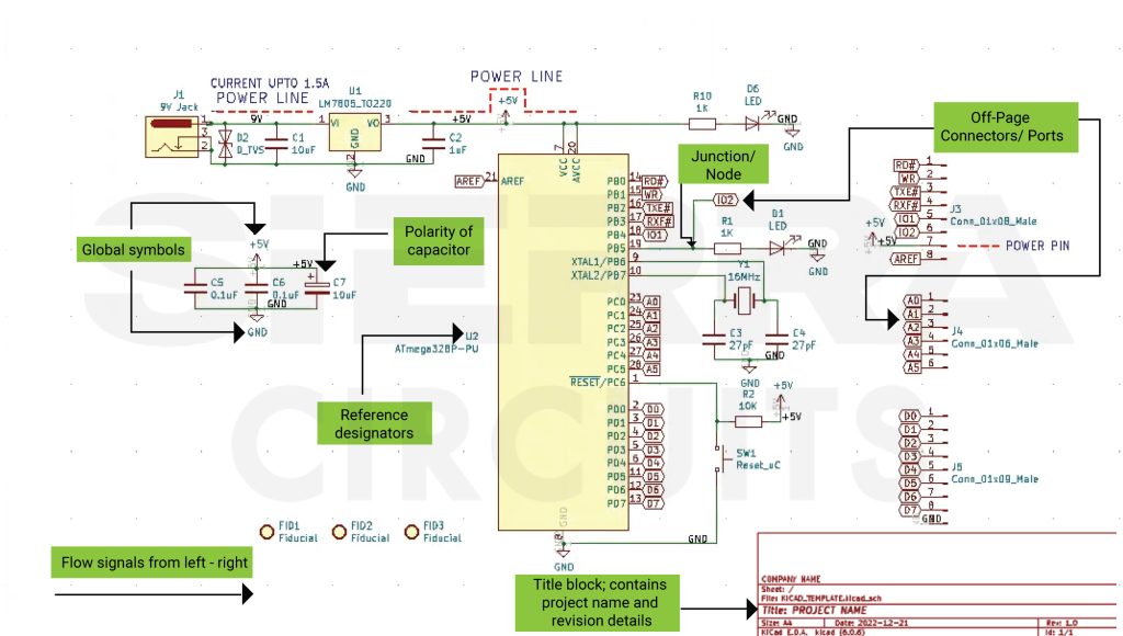
The next important part of the electronic circuit design process is to draw the schematic diagram using EDA tools like Altium, KiCAD, and Cadence Allegro. These tools provide several features like schematic capture, creating electronic components, simulating complex circuit functions, and BOM creation. They also include PCB layout packages, component footprints, 3D views, and output of manufacturing files. Choose an EDA tool that is comfortable and provides adequate design support.
Capturing the schematics forms the basic foundation on which the rest of the design documents are built. There needs to be information synchronization between the schematic, netlist, and layout. For the best schematic design practices, see how to draw and design a schematic.

Design for Manufacturing Handbook
11 Chapters - 96 Pages - 90 Minute ReadWhat's Inside:
- Annular rings: avoid drill breakouts
- Vias: optimize your design
- Trace width and space: follow the best practices
- Solder mask and silkscreen: get the must-knows
Download Now
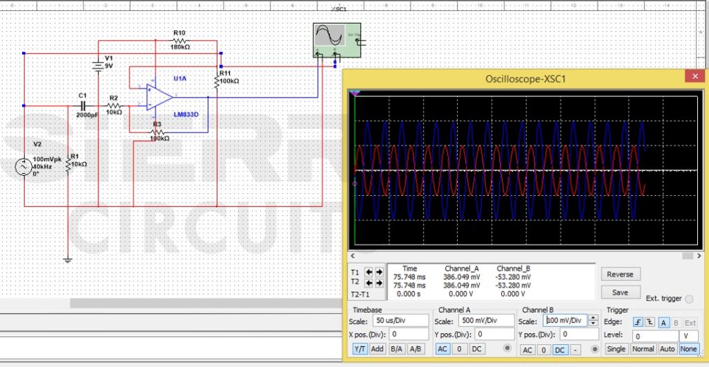
8. Carry out simulations and functional tests
Verifying and testing individual circuit blocks of the design that are critical using simulation software is the next step in electronic circuit design. Many EDAs provide this option, where the correct functionality of the block can be tested. You can make necessary changes in case the circuit doesn’t function as per requirement.
Simulation software has limitations, and sometimes a good circuit may not provide accurate results on the system. Therefore, it is recommended to rig up the circuit section physically on a breadboard to test its functionality. If there are any errors in any circuit block, you can troubleshoot and rectify the issue in the next design iteration.
Another very important design practice is to document every step of the design process. This includes all details like reasons for choosing a solution, a component, a logic table, and undertaking special considerations.
The advantages of keeping notes are:
- Efficient resolution of design issues
- Better solutions for the current design based on previous works
- Easy knowledge transfer across teams.
After simulations and functionality testing, you can now route the PCB layout. Appropriate footprints need to be used/created for the parts and linked to the component before generating the netlist. The netlist is then imported to a layout editor for routing.
You need to ensure effective component placement and grouping to facilitate optimized routing. This should be done by taking into consideration the power, thermal, and electrical variations of the circuit. See mastering the art of PCB design basics to learn about stack-up preparation, footprint inspection, routing, fabrication, and assembly drawings. It also gives an overview of the DFM and DFA quality checks that are carried out for manufacturing a good-quality PCB.
To turn your PCB concept into reality, read building a PCB prototype from scratch: A designer’s guide.
Need help in designing reliable PCBs? Our engineering team can help you with thermal management, stack-up design, and DFM analysis.
You can book a meeting with our experts or call us at +1 (800) 763-7503.

Key takeaways:
- Effective electronic circuit design practices are essential for building well-planned circuit boards.
- Block diagrams help define specifications and component groupings, facilitating a divide-and-conquer strategy in circuit design.
- Proper placement of decoupling, coupling, and bypass capacitors is critical to stabilize power supplies and prevent signal interference.
- Pull-up, pull-down, and zero resistors are used to maintain logic levels in digital ICs and enable circuit modification and troubleshooting.
- Utilizing microcontrollers and mixed-signal circuits can enhance circuit performance efficiency and reduce component count.
- PWM signals can be used to reduce power consumption, particularly in battery-operated circuits.
- Strategic signal return paths and grounding techniques help prevent EMI and ground loops.
- Safety measures such as ESD protection circuits, reverse polarity, transients, and over-voltages are crucial for circuit reliability.
- Component selection should consider datasheets, obsolescence, derating, and overrating, while using standard values and avoiding long lead times.
- Capturing schematics and verifying them using EDA tools, followed by simulations and functional tests, are essential for verifying circuit performance.
- Documentation is essential for efficient issue resolution and knowledge transfer across teams.
- By following these practices diligently, engineers can design efficient and reliable electronic circuits, ensuring optimal performance and longevity.
Designing electronic circuits can be a daunting task, but if these practices are followed diligently along with correct documentation, you will be able to hone the necessary skills. Share your best electronic circuit design practices, experiences, top tips, and your queries on our SierraConnect forum.


