


Contents
An extensive PCB design checklist proves beneficial for reviewing the requirements of a circuit board. Depending on the board specifications, the parameters in the checklist vary.
A lot goes into the development of a circuit board. Misplacement of a single element might lead to unexpected errors. You have to perform specific checks before proceeding to the next step to avoid board respins.
In this article, we will focus on multiple PCB design checks that are essential to building a circuit board. Take a print copy if required and refer to this checklist during or even after your design phase.
The checklist a designer needs
The primary assessments that should be considered for a quality board layout are discussed below:
- Mechanical checks
- Drill checks
- Component placement checks
- Routing checks
- Solder mask and solder paste checks
- Verification of silkscreen
- Fab note checks
- Production file checks
- BOM checks
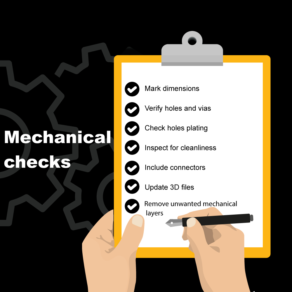
Mechanical checks
- Verify the dimensions of the bare board.
- Check the holes and vias from the drill chart.
- Mounting hole dimensions from the edge of the board and the hole-to-hole dimension.
- The default size of mounting holes should be 3.3 mm. Generally, the hole size should not be less than 3.3 mm.
- Mounting holes and NPH (non-plated holes) should have anti-pads (clear copper area).
- The head of the screw, which is a screw head/nut size, should be 40 mils greater than the hole diameter.
- Inspect the plating details, such as the thickness and the status (whether the hole is plated or non-plated).
- Remove unwanted stubs and check if any overlapping silkscreen occurs.

- Verify the connector position and arrangements.
- Examine the 3D file to have a 3D view of the placement and arrangement of the components by rotating and moving the cursor in different directions.
- Remove unwanted layers, often added to the design by the tool.
Drill checks
- Send the latest/updated drill chart to the manufacturer.
- The drill chart should have separate drill symbols for each drill size.
- Use “+” for vias
- Square with alphabet for plated holes
- Triangle with alphabet for non-plated holes
- Ensure the drill chart shows
- ±3 mils tolerance for plated holes
- ±2 mils tolerance for non-plated holes
- Tolerance for vias can be adjusted depending on the via drill and pad size. Typically, via tolerance is set to ±2 mils.
- Check if all the drills are whole numbers.
- Verify if each drill matches the desired value.
Component placement checks
- Generate the 3D files and check if the component and connector directions are correct. Place the mating 3D model connectors on the PCB connectors and ensure that they fit properly and there is enough space between the connectors.
- Place decoupling capacitors near power pins.
- Verify whether ESP components are placed close to connectors or not.
- Include series resistors close to the source to avoid EMI.
- Design the power supply systems as per the datasheet guidelines.
- Add signal names for connector pins wherever possible.
- Check whether the connector footprints’ place bound is bigger than the mating connector of the board connector. Sometimes, the mating connector is bigger than the PCB connector.
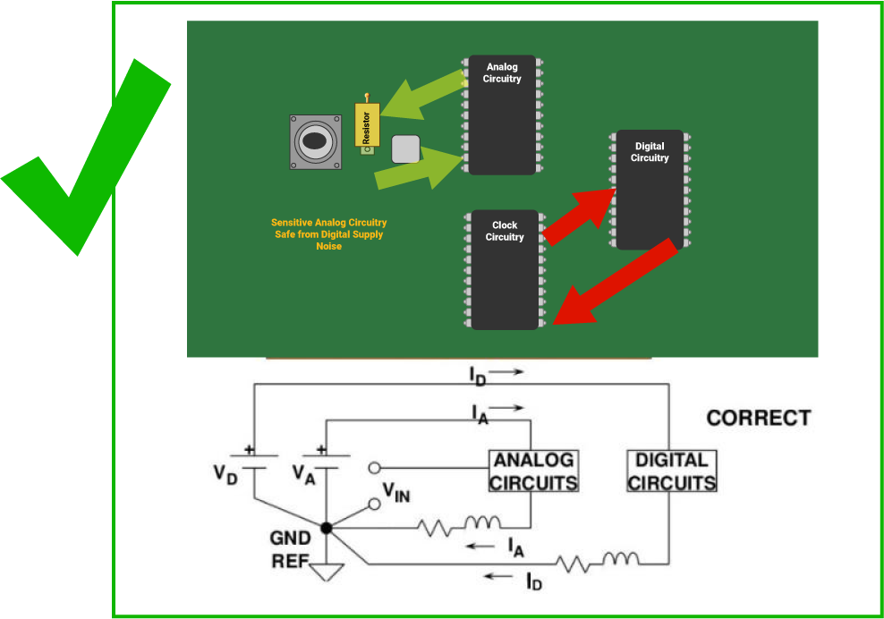
- Ensure analog and digital circuits are away from each other.
To find out more about failures in components, read common errors encountered in discrete components.
Routing checks
Routing should be 100%.
- Trace width: It helps you to find out the impedance and the current-carrying capacity of the traces.
- Trace spacing: It helps to suppress crosstalk and maintain controlled impedance on different signals. Trace spacing also depends on copper thickness, for instance, 8 mils trace spacing is required for a 2-ounce copper.
- Length matching tolerances: This ensures that the skew is within acceptable limits.
- Routing topology: Check the routing topology on the critical nets.
- Via count: A certain amount of loss and reflections are present on every via or an interconnect, particularly on impedance-controlled traces for high-speed signals. Via count should be limited to a small number to avoid signal distortion. Back-drilling is a suitable approach to prevent the stub in the transmission line at very high bandwidths on high-speed nets.

High-Speed PCB Design Guide
8 Chapters - 115 Pages - 150 Minute ReadWhat's Inside:
- Explanations of signal integrity issues
- Understanding transmission lines and controlled impedance
- Selection process of high-speed PCB materials
- High-speed layout guidelines
Download Now
- Check for unrouted nets by running the DRC (design rules check).
- Practice good routing skills:
-
- Keep the signal paths short and direct.
- Ensure the CI signals are routed at the correct width and space and on the correct layers.
- Isolate clock lines and other sensitive traces to avoid crosstalk.
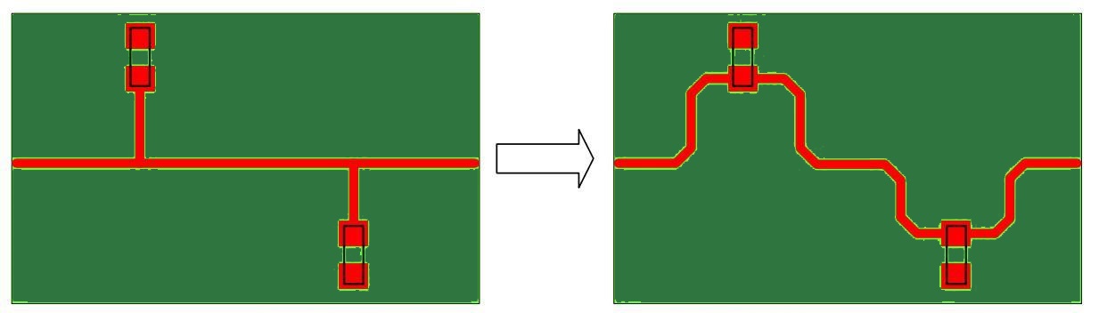
- Avoid broadside coupling by routing adjacent layers with alternating horizontal and vertical traces.
- Complete the differential pair routing with correct spacing.
- Check for the relocation of any traces routed across split planes.
- Short the traces connected to decoupling capacitors.
Solder mask and solder paste checks
- Check that all SMD components have defined solder mask and solder paste.
- Verify that the through-hole components have solder mask.
- Ensure an 8 mil (minimum 5 mils) solder mask bridge is configured under DRC.
- The exposed center pad of QFN ICs should have solder paste in small patches.
Verification of silkscreen
- Verify the revision number, date, and blank space for a serial/assembly number for silkscreens.
- Check the labeling of the connector pin-out, functional groups, and high-density chips.
- Include the fuse size and type on the board.
- Label the LEDs, buttons, mounting holes, and jumpers.
- All legend text should be of the same size and read in one or two directions.
| Board category | Height in mils | Width in mils | Trace in mils |
|---|---|---|---|
| Low density | 65 | 45 | 6 |
| Medium density | 35 | 25 | 5 |
| High density | 25 | 22 | 5 |
- Check that all polarized components have a polarity marking and are clearly visible.
- Ensure all the ICs have pin1 indications and are clearly visible.
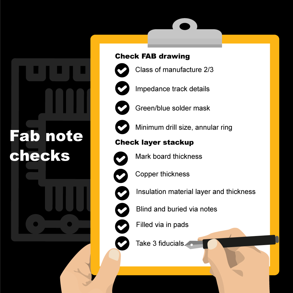
Fab note checks
Fabrication notes should include:
- Fab drawing:
- Class (IPC class 1/2/3) of the board is mentioned.
- Impedance track details layer-wise.
- Color of the solder mask (blue/green).
- Minimum drill size and the details of the annular ring
- Layer stack-up:
- Mark the board thickness.
- Copper and dielectric layer thickness.
- The insulation layer and material name, and thickness.
- Add notes on blind and buried vias (number of vias and the layer details)
- Mention details about via filling, especially for via-in-pads in BGAs.
- Fiducial points (minimum 3 fiducial points).
Production file checks
These files include the centroid file, bill of materials (BOM), netlist file, and Gerber files. Perform the following checks to ensure error-free production files.
- Validate the number of the inner layers and the position of the power and ground planes.
- Check the numeric-controlled (NC) drill file, which refers to the information regarding the size and location of the via and hole drilling.
- Validate the pick and place file to assemble the SMT and the through-hole components accurately. This file requires the following information:
- Component reference designator.
- The X-Y coordinate of the component centroid.
- The direction of the rotation of the components in degrees (clockwise rotation indicates a positive value, and anti-clockwise rotation indicates a negative value).
- The side of the board on which components need to be placed (top or bottom).
- Inspect the IPC-356 netlist file that contains the pin number, net names, and X-Y coordinates of starting and terminating points. This file is based on Gerber and drill data and formatted in ASCII text.
- Verify the ODB++ file that is crucial to exchange data among CAD, CAM, and manufacture of the board.
- An alternative to ODB++ is IPC 2581. There are free IPC 2581 viewers to double-check your data. With IPC 2581, all the files a PCB fabricator and assembler need are included in the data package.
- Examine the APR lib file. This is an aperture library file of Altium Designer to help designers draw and simulate the circuits.
- Check the EXTREP file, which is the extension report file of Altium.
- Create a PDF document including the following details:
1. Top and bottom assembly.
2. Fab drawing.
3. Drill drawing. - Include a readme file that contains 24-hour contact information, any known issues like intentional opens and shorts, and any special concerns like overall board thickness, tolerance, etc.
- Request your manufacturers to send the final Gerbers for approval. This is especially important on re-orders that may have gone through design changes.

BOM checks
- Check if the DNI components are marked in the BOM. Make a separate list at the bottom.
- Check the material list and give your approval to the manufacturer.
- Ensure you send the updated (latest) BOM file to the fabricator. Sometimes designers make changes in the design and forget to update the BOM file. So keep track of the changes and inform your manufacturer.
- Check for obsolete and out-of-stock components and be ready with an alternate component.
It seems a great reward when you finally get the desired board after a rigorous effort. In the entire PCB design and assembly process, it is essential to follow a checklist. This helps you in creating a high-quality circuit board and also saves time. Please let us know in the comments section if you require any assistance in designing your circuit board.
You can book a meeting with our experts or call us at +1 (800) 763-7503.

About Poulomi Ghosh : Poulomi is a microwave engineer specializing in EMI, EMC, RF, and high-speed electronics. As a senior technical writer at Sierra Circuits, she creates advanced engineering articles and webinars for hardware engineers and PCB designers.


Start the discussion at sierraconnect.protoexpress.com