Contents
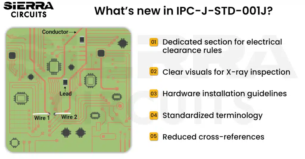
PCB land pattern defects should be treated with due attention since their design is very essential for the PCB manufacturing process. Land patterns and footprints in a PCB are often treated as similar terms. But they are not the same thing.
Footprint gives an idea of the actual size of the component. For example, when we put a component on the sand, it will leave its impression there. This imprint is its actual physical size. On the other hand, we use the term ‘land pattern’ when we want to define the size of the pads and the outline of the component that needs to be soldered onto the PCB. One important thing is that the component may have multiple land patterns on producibility levels and tolerances associated with fabrication and assembly processes, but it can only have 1 single footprint.
This webinar was conducted to identify some PCB manufacturing issues caused by land pattern defects. We have also covered some real-time solutions to avoid land pattern defects. So, this was the agenda during the presentation:
- What are footprints and land patterns?
- Manufacturing defects caused by land patterns
- Tips for creating high-quality land patterns
- How to leverage automated verification
- SnapEDA and Sierra Circuits
About the presenter: Elizabeth Bustamante, CAD Manager at SnapEDA, manages a team of 11 electrical and mechanical engineers. She and her team create thousands of CAD libraries per week for around 1 million engineers through SnapEDA. SnapEDA helps users to design their symbols and land patterns to ensure proper PCB manufacturing.
We have curated a set of questions and answers taken exclusively from our webinar on land pattern defects. This provides a manufacturer’s perspective to the PCB designer. You can also view the entire webinar here.
Q1: How can we decide whether a given drill is Plated Through-Hole (PTH) or Non-Plated Through-Hole (NPTH) if it is not mentioned in the datasheet? Does it make any difference if we took PTH instead of NPTH or vice versa?
Elizabeth Bustamante: PTH is used for soldering a component to the PCB. It involves an electrical connection, something that does not happen with NPTH. If the datasheet does not mention anything about it and you don’t fully understand the connections of your pins, you should contact the component manufacturer directly.
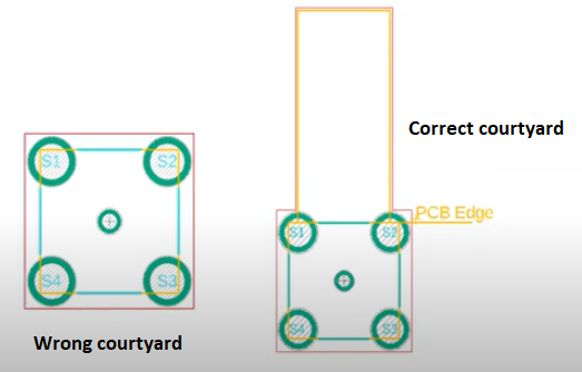
Q2: What drives the boundary of the courtyard excess?
Elizabeth: When we talk about the courtyard, we need to mention that there are two terms. One is a contoured courtyard, and the other is courtyard excess. The contoured courtyard provides the minimum electrical and mechanical clearance around the combined component body and your land pattern boundaries. The courtyard excess provides the clearance between the rectangle containing the land pattern and the component and the boundary of the contoured courtyard.
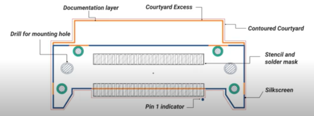
The courtyard excess can be designed following the IPC-7351B standard. For example, a SOT package can be created following IPC density level B, and it is recommended to design this land pattern following a 0.25mm courtyard excess.
Q3: Tombstoning also happens due to land pattern defects, correct?
Elizabeth: Yes, from the perspective of land pattern defects, it can be caused by pads with different sizes, and this usually affects SMD-2 packages.
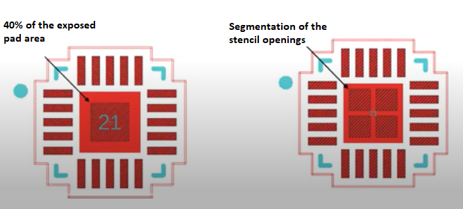
Q4: How does the land pattern determine the amount of solder paste? Is it just that the bigger a pad is, the more solder paste will be used? So, the general recommendation is to make large pad sizes?
Elizabeth: Not necessarily. We follow IPC-7351B paste mask standards. IPC recommends to follow a 1:1 ratio between the copper pad and the paste mask. However, for exposed-pad packages like the QFNs/QFPs, if the exposed pad is a square above 4 x 4mm then the paste mask should be segmented into a symmetric pad array. This design recommendation enables the component to settle to the pad better, rather than floating on top of the solder paste. If the exposed pad is a square below 4 x 4mm then the default paste mask for these thermal pads is 40% of the overall land area. In the end, either the printed board assembler or the designer can modify the information provided for openings in the stencil to meet the specific solder volume requirements. You can read IPC-7525 for more information. For example, they recommend 50%-80% instead of 40%.
Q5: If one pad of the two-terminal components is part of a large copper pour (i.e., ground plane) and the other pad ends in a standard trace, would this cause tombstoning?
Elizabeth: Yes, it could cause tombstoning. For example, if one of the pads is connected on one side to a large and thick ground plane and the other pad is connected to just a small trace.
Q6: SMT inductors always seem to be a problem, since the pads are on the bottom, not the edges. Any suggestions to improve this?
Elizabeth: Whenever we design a footprint, before understanding the type of footprint that we are designing, we evaluate different parameters that are important for designing that land pattern. For SMT inductors, choose between an IPC compliant package or the PCB land pattern recommended in the datasheet. Try to follow the last one if you don’t know how to properly categorize the package type.
Q7: How do you get around the potential problem of having floating components on a PCB?
Elizabeth: The main cause of this problem is poorly designed solder paste stencil. You can solve it by desoldering the floating component followed by soldering the component manually after removing the excess solder. It is not 100% feasible, but you can try it.
Q8: Can you please tell me the IPC standard for stencil design?
Elizabeth: It is IPC-7525A.
Q9: Do you have any recommendations for wireless modules (LCC or LGA) to avoid soldering problems?
Elizabeth: For fine-pitch LGA packages, you can check the guidelines defined JEDEC 95, 4.25. They recommend that for NSMD packages, the solder mask opening should be 0.075 mm larger than the solder ball pad, and there are more important recommendations too. For LCC packages, if the component manufacturer does not have any recommendations then you can take a look at IPC-SM-782. It has some land pattern recommendations including tolerances.
Q10: For SMT hand soldering, is it recommendable to use Level A or bigger sizes?
Elizabeth: Although there are many parameters to consider, if you are going to manually solder your components then try to choose large pitch sizes. But yes, it is always wise to make your pads bigger for easier hand soldering. You could try to follow Level A, but please consider that this level was developed to accommodate wave or flow solder of leadless chip devices along with leaded gull-wing devices.
Q11: During the SMD assembly process, in some of my 0603 resistors, one pad is not soldered, it is open. Is it any design issue?
Elizabeth: Did you receive more information about what caused it? Could it be tombstoning? It would be great to look at the land pattern you designed and understand what went wrong. From the land pattern side, please review the pad sizes, your mask openings, and stencil design.
Q12: For annular rings, do you know if there exist any standard for the relation between drill holes and the annular ring?
Elizabeth: The standard is IPC-2221A. For a more detailed explanation, read the annular ring explained by a PCB manufacturer.
Q13: How to design proper solder mask opening clearance?
Elizabeth: It mainly depends on your fabrication house specifications. But as a general recommendation, it is common to have around 2-3mils clearance between the pad and the mask. You can also set the rules based on your PCB manufacturer requirements and validate them while you run your DRCs.
Q14: I am planning to use castellated pads around the edge of a PCB. What issues do I need to watch out for, and how do I convey this to the PCB manufacturer?
Elizabeth: You need to understand your EDA tool limitations. Does it natively support castellated pads? If not, try to find a workaround, there are many methods. You could check the layer that handles the outline cutouts (milling layer in Eagle) in the board is properly set and whether you are designing outlines using that layer. You could also add a solder mask extended at least 0.1mm away from the copper and check that the stencil size is the same as the copper pad size (top and bottom). Also, check if your fabrication house understands what you have designed and/or if you need to update your current design to meet their requirements.
Q15: In an HDI design, sometimes the silkscreen of the components collides to save space. If a design is necessary to do this, could this be inconvenient while manufacturing the PCB?
Elizabeth: Yes, it can affect your PCB while being manufactured, but you could easily prevent it from the library design stage. You can add a keep-out area that is at least 0.3 mm apart from the silkscreen region. For very small components like (0203 resistors), it is better to remove the silkscreen in order to prevent issues at the soldering stage. Read more about the importance of high-quality PCB libraries.

HDI PCB Design Guide
5 Chapters - 52 Pages - 60 Minute ReadWhat's Inside:
- Planning your stack-up and microvia structure
- Choosing the right materials
- Signal integrity and controlled impedance in HDI
- Manufacturing considerations for higher yields
Download Now
Q16: What is the business model for SnapEDA?
Elizabeth: All our schematic symbols, PCB footprints, and 3D models are free for our users. We work directly with the component manufacturers to offer engineers high-quality content and to help them design their products faster.
Q17: Does an inductor having dot marking on it make a problem if we rotate it on PCB?
Elizabeth: You need to make sure that the polarity marking is in the silkscreen layer and make sure that you also know where your pin 1 is located. It is highly important to place the component properly on a PCB. For inductors, it is not a common problem, but I have seen some inductors with polarity marking, like Murata’s inductors. At SnapEDA, we usually add a dot as a polarity indicator. Read more on how to place components in KiCad?
Q18: Are there any land pattern design considerations that one must take into account regarding EMI/EMC?
Elizabeth: To avoid land pattern defects. you need to double-check your pin directions/types when wiring your components. You could introduce connection errors by having wrong pin directions in your symbols. You could misunderstand the function of a pin and ended up having electrical connection problems.
Q19: Sometimes in SnapEDA, appears like 3 different options for the same device, but sometimes in one of these 3 different options, appear the official logo from the manufacturer. Does this mean that it is an official device from the manufacturer?
Elizabeth: Yes. You are talking about the information available on each part page. We show three different messages to our users to provide more information about where the part has been taken. Suppose we are working with a component manufacturer, say, Murata, TE Connectivity, or Samtec, we add their logo over there and share that they have reviewed and approved the component files. In another situation, where the component manufacturers upload their files, you will see a message that says that it was created by that component manufacturer and not by the SnapEDA team. If the component is specifically designed by the SnapEDA team, you will see only our logo in the uploader information.
Q20: Does SnapEDA prefer to design footprints using mm or mils units?
Elizabeth: We usually design land patterns following mm units. That is because of the datasheets we use to get the information. Most of them are in mm units.
Q21: Could you please give a little info about the hole diameter in the press fit components?
Elizabeth: We usually follow the manufacturer’s land patterns and their recommended drill hole sizes and diameter. But as I mentioned before, there are two IPC standards (2221/2222), which I recommend to calculate hole diameters. IPC also developed a new standard: Press-Fit for Automotive Requirements and Other High-Reliability Applications (IPC-9797).
Q22: Could all of your components be imported in KiCad and be used for free?
Elizabeth: Yes, they can be used for free, but you can not import all of them simultaneously in KiCad. You will have to download a big batch. We allow users to download 30 parts per day. Read more on how to export Gerber and other production files in KiCad.

Q23: Could you please elaborate a little about the zero-component orientation? What is it useful for?
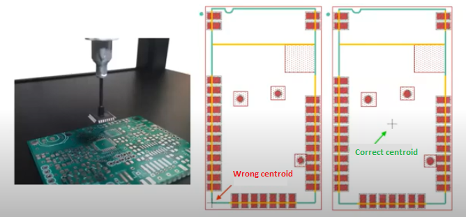
Elizabeth: Zero-component orientation indicates the rotation around which the land pattern is built. It is very important to pick and place assembly lines. Zero-component orientation depends upon the IPC standards that you are going to follow and the density level too.
It is advised not to mix the level and standards, and it is better to contact your fabrication house. Always ask them if they have a pick and place assembly. Do they have any limitations? You can also ask them if sending the centroid of the land pattern would be enough. Or, if they want all component orientations to be defined following a specific standard.
Q24: What difficulty do we face in assembling 01005 packages?
Elizabeth: Tombstoning and bridging are the common defects in the assembly of 01005 components. From the perspective of land pattern defects, it is important to follow the manufacturer’s recommended layout. If possible, the ratio between the stencil aperture for solder paste release and the pad area should be 1:1. And it is recommended that the solder mask is defined in between the pads.
Q25: Can you highlight on pad vs hole size ratio for a through-hole pin in high volume manufacturing. Does this vary on board thickness?
Elizabeth: Yes, it does. Based on IPC, the size of the via holes should be selected based on the printed board thickness versus the hole diameter or aspect ratio limits as defined by the printed board fabricator. You can refer to the Industry Standard for Printed Board Design (IPC-2221). And I also recommend you to check with your fabrication house what their aspect ratio is for standard drilling and if they have any specifications for high-volume manufacturing. Read our blog on 6 DFM issues.

Q26: How much weight should we give to manufacturers’ recommended land patterns compared to IPC 7351?
Elizabeth: It mainly depends on the package type. For standard packages, I would recommend you to follow IPC standards, however, there can be exceptions for isolators, TVs, or any other high-voltage packages. You could follow the manufacturer’s recommended land pattern if it’s available. For non-standard packages, it is better to follow the manufacturer’s land pattern, and if it’s not available, you can try to calculate the drill hole sizes/diameter using the IPC-7351 standard. You can also follow the mechanical dimensions including the tolerances and the courtyard excess.
Q27: What would be the most common defect you see with people’s footprints? Or what would be something easy to lookout?
Elizabeth: The most common issue that we see in footprints is related to pad sizes. For example, sometimes people do not know what standard to follow when creating a footprint. When our users request us to create footprints, we design them after considering a lot of different design parameters but mainly if it’s an IPC package or not. We deliver the design, and our customers get back to us saying: Why did not you follow the recommended footprint layout? Or, why are you following IPC standards? It is not that easy to understand initially. It becomes easier after seeing thousands of datasheets, land patterns, manufacturing more and more PCBs, and perceiving the primary parameters that will help you choose the best method and standard for your land pattern design.
Q28: What is the difference between non-solder mask defined (NSMD) and solder mask defined (SMD) in a land pattern?
Elizabeth: NSMD pads have the solder mask opening larger than the pads, and SMD pads have the solder mask opening smaller than the copper pad.
Q29: For any component with unusual pin mapping, I write in my instructions to the PCB layout designer that the pin numbers have to be shown in the silkscreen. Then I check the silkscreen against the manufacturer’s drawing. Is this as much for the benefit of test technicians’ hand-probing the board as for my layout check before sign-off?
Elizabeth: I’d try to leave those types of instructions on the documentation layer, and I’d have only polarity markings and just everything specifically serving as a reference indicator for placing the component on the PCB.
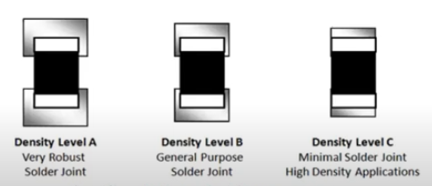
Q30: What conditions must be met for a board designed at IPC 7351 level C to be manufactured successfully?
Elizabeth: It depends on your design goals. If you’re designing a high component density PCB, you may want to go with Density Level C: Minimum (Least) Land Protrusion, then you can consider product qualification testing based on the conditions shown in Table 3-24 in IPC-7351B, and finally, you can adapt your land pattern geometries for the density level you chose.
Q31: How can we get the footprint from SnapEDA’s Library?
Elizabeth: You can go to SnapEDA’s official page, search for the component that you want to integrate into your design. If it’s not available, click on ‘Notify me when available’ in case, you want to request it for free.
PCB footprints and land patterns are largely overlooked, but they are the fundamental step in the design process. Often, engineers do not realize that their manufacturing defects may be caused by poorly designed land patterns. To avoid the chances of footprint/land pattern defects, one must be aware of the IPC standard limits. Running a proper DRC and ERC check also helps for accurate board designing. Calculated solder paste amount, exact stencil-design, and automated verification help both users and manufacturers in realizing a defect-free PCB. Set your own diagnostic rules for silkscreen clearance, pin 1 indicator, the centroid of the components, and etc. Always try to understand your PCB requirements and the usage of good CAD libraries to avoid land pattern defects.

Design for Manufacturing Handbook
11 Chapters - 96 Pages - 90 Minute ReadWhat's Inside:
- Annular rings: avoid drill breakouts
- Vias: optimize your design
- Trace width and space: follow the best practices
- Solder mask and silkscreen: get the must-knows
Download Now