Contents

On-demand webinar
How Good is My Shield? An Introduction to Transfer Impedance and Shielding Effectiveness
by Karen Burnham
Microwave PCB design presents unique challenges that differ from lower-frequency boards. At microwave frequencies (1 GHz to 30 GHz), the short wavelengths and high signal speeds introduce impedance mismatches, signal loss, crosstalk, and EMI.
The demand for microwave and RF PCBs is rapidly increasing, presenting significant growth opportunities in both global and U.S. markets. For statistics, see antenna integration and RF design guidelines for 5G PCBs.
When designing printed boards for microwave frequencies, addressing parasitic elements, managing the skin effect, and controlling transmission line behavior become critical. These factors complicate the design process, as small variations in layout can lead to performance degradation.
The image below shows the EM spectrum. It comprises all forms of electromagnetic radiation, ranging from radio to gamma rays.
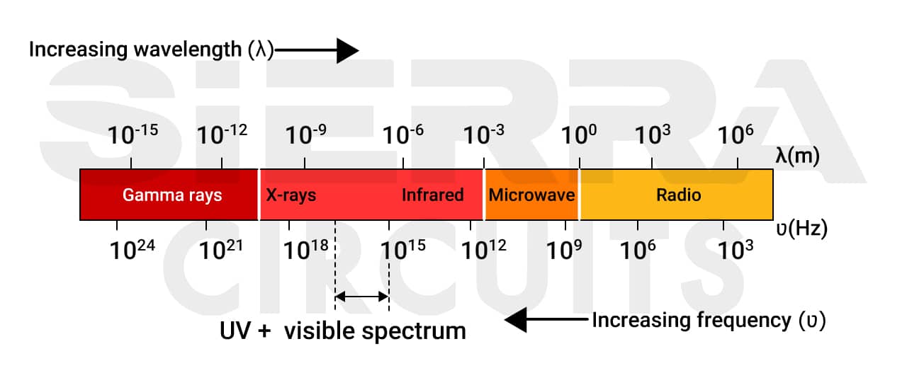
In this blog, you’ll learn the common microwave PCB design challenges and how to overcome them.
Highlights:
For a robust microwave PCB:
- Employ matching circuits near both the source and load to maintain consistent impedance.
- Maintain a minimum spacing of 3W between controlled impedance traces.
- Implement a dedicated ground plane for each RF layer.
- Incorporate board-level shielding around sensitive components.
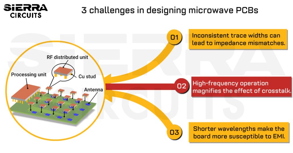
1. Inconsistent trace widths can lead to impedance mismatches
Maximum power transfer occurs when the trace impedance matches the characteristic impedance (50Ω). Therefore, it is crucial to match these impedance values to ensure efficient power transfer from the source to the load. Matching circuits are employed to align the measured impedance with the characteristic impedance.
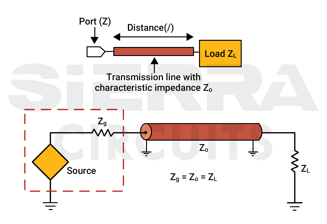

However, the measured impedance at different points in a microwave circuit can vary with distance from the source or load.
To ensure consistent impedance matching, the impedance should remain unchanged regardless of the distance from the source/load. Consequently, matching circuits must be placed near both the source and the load to maintain this consistency.
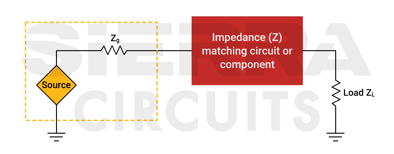
A matching circuit is intended to adjust the impedance of a circuit to align with its characteristic impedance. It utilizes reactive components like inductors, capacitors, and RF stubs.
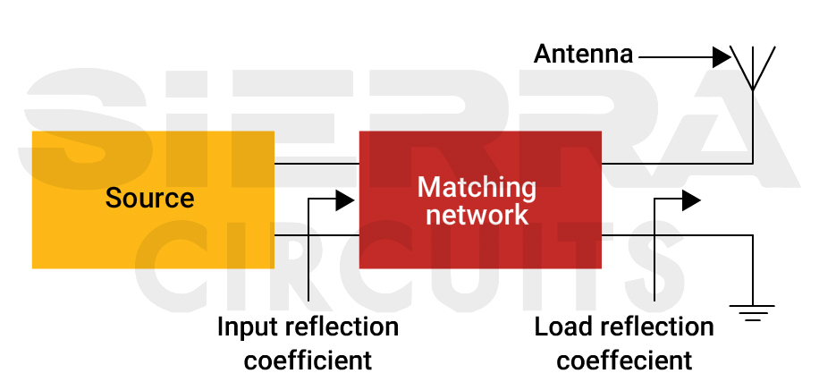
High-speed digital signals have some tolerance for impedance mismatches, but as the frequency increases, this tolerance decreases.
RF & Microwave Design Guide
8 Chapters - 44 Pages - 60 Minute ReadWhat's Inside:
- Basics of RF and microwave board design
- Choosing RF materials
- Trace, grounding, via, and stack-up design
- Component selection and placement
- Testing and isolation requirements to avoid interference
Download Now
2 critical factors to consider when addressing impedance mismatches
1. Skin effect loss
You can employ various techniques and strategies to mitigate this issue. One common approach is maintaining the trace thickness less than 0.1 times the material’s skin depth.
To learn how to choose the right dielectric material for microwave boards, see microwave PCB material selection and CPW for signal integrity.
2. Microwave signal trace length
The probability of signal loss increases with the length of the signal lines. Ideally, these traces should be maintained at 1/20 of the wavelength. If they extend beyond 1/16 of the wavelength, known as the critical signal length, impedance control using inductors and capacitors (matching circuits) must be applied at the line’s termination.
7 strategies to design matching circuits for microwave circuit boards
- Measure impedance at the exact points where the microwave and radio frequency components are to be placed.
- Never use the L network for circuits operating in gigahertz frequencies. Instead, opt for a PI or T-matching network.
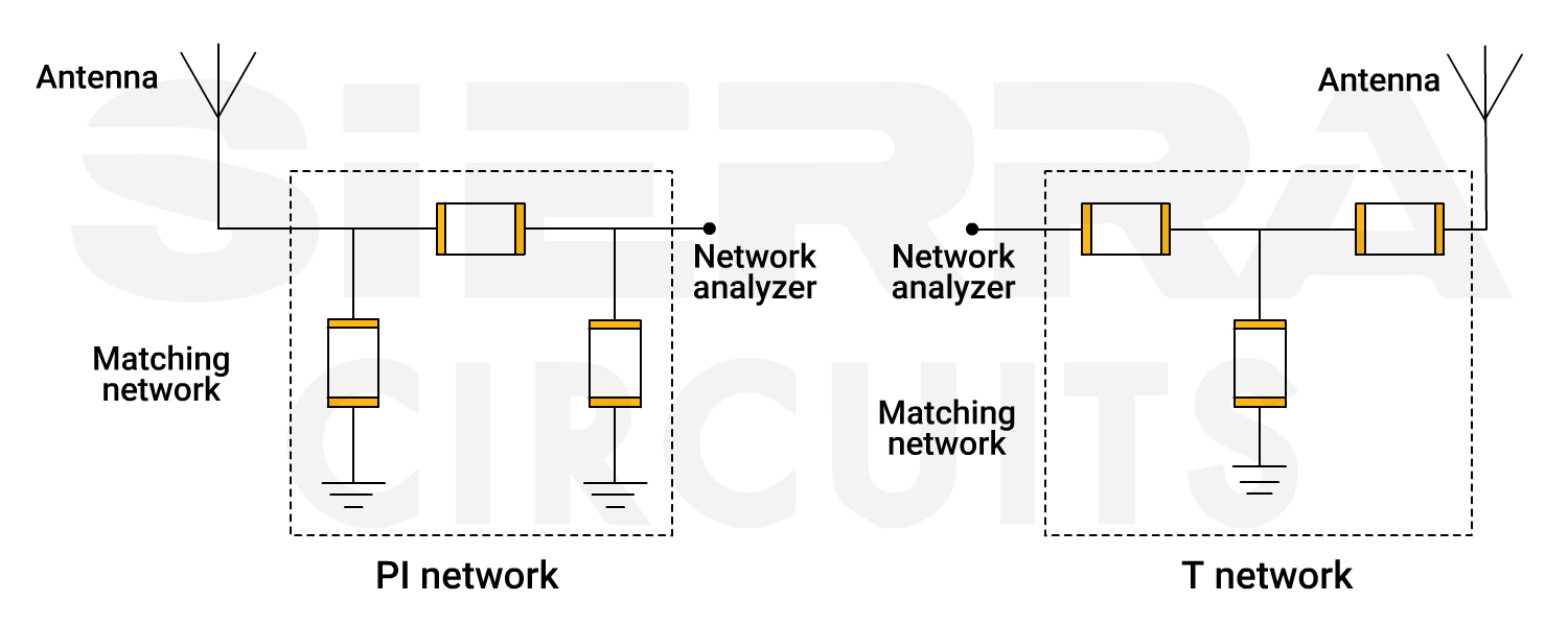
PI and T matching network topologies in microwave PCB design. - Do not use connectors to connect the shunt components. It is better to place the components on the trace itself.
- Choose components with high-Q values for capacitors and inductors.
- Ensure the series resonant frequency of capacitors is twice the operating frequency.
- Make sure the self-resonant frequency of inductors is twice the operating frequency.
- Use intentional stubs strategically for impedance matching in your RF circuits while minimizing unintentional stubs to avoid increased circuit attenuation.
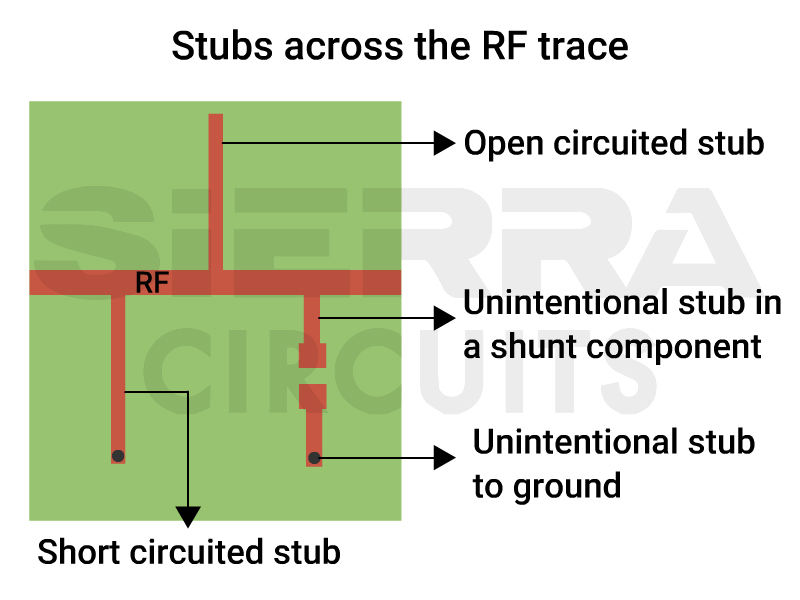
The input impedance of a stub can be either inductive or capacitive, depending on its electrical length and whether it is open or short-circuited. Shorter operating wavelengths result in shorter stubs. In microwave frequency designs, the shorter wavelengths make stubs conveniently small.
2. High-frequency operation magnifies the effect of crosstalk
Crosstalk in high-speed PCBs occurs when excess voltage or current from one trace induces unwanted effects on another trace, even without any physical connection. The coupling effect in microwave PCBs refers to unintended signal interactions that become prominent at higher frequencies.
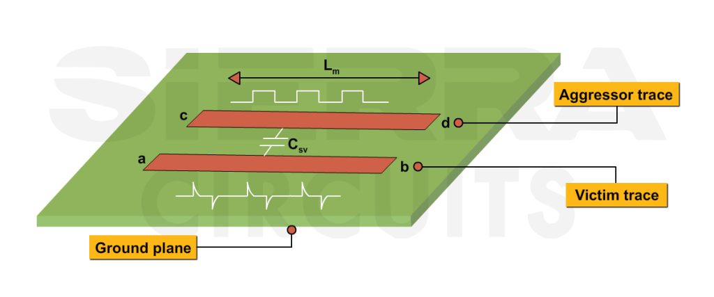
This phenomenon includes various types of interference, such as capacitive and inductive coupling, particularly in closely spaced traces, shared ground planes, or adjacent components.
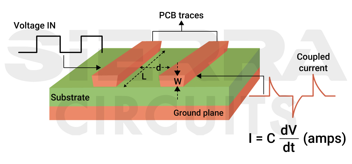
This issue presents significant microwave PCB design challenges because of its direct correlation with the edge rates of the active line. As PCB densities increase, the problem of crosstalk becomes more critical.
High-frequency transceivers, commonly used in microwave boards, are particularly vulnerable to crosstalk due to their intricate architecture.
Typically, this architecture includes a high-output-level local oscillator (LO) paired with a frequency mixer, along with RF and IF (intermediate frequency) amplifiers to enable frequency conversion.
The LO often relies on a tunable oscillator, such as a voltage-controlled oscillator (VCO) or a yttrium iron garnet (YIG) oscillator. These oscillators can radiate or leak signal energy, which nearby transmission lines could conduct.
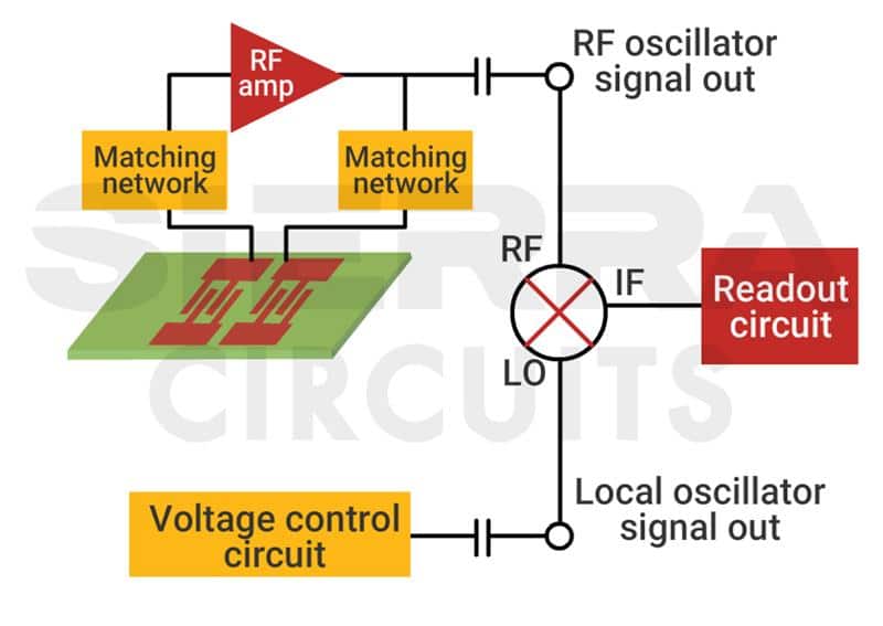
Additionally, closely spaced parallel transmission lines in compact circuitry act like antennas, picking up signal energy from high-energy sources like the LO or nearby lines. This unintended signal energy can conduct into components, such as amplifiers, amplifying crosstalk signals, and potentially degrading transceiver performance.
Mitigating these coupling effects requires strategic design practices, including appropriate trace spacing, ground plane isolation, and controlled impedance implementation.
Designing a microwave circuit board? Check out our PCB design support.
18 tips to mitigate crosstalk in your microwave board
- Place power and ground layers in the inner PCB layers to act as shields and reduce signal trace lengths, thereby minimizing cross-interference between signals.
- Maintain proper spacing between impedance-controlled traces and components. Further, keep a minimum distance of 3W between adjacent traces.
- Increase the spacing between traces overlapping in multilayer circuits to reduce or minimize crosstalk. While this may hinder miniaturization, finding the right balance is essential.
- Separate signal traces such that the distance from center to center is a minimum of 4W to reduce mutual coupling.
- Decrease the dielectric spacing between a signal line and its reference plane to lower the potential for crosstalk.
- Introducing a co-planar structure by inserting a ground plane between traces to provide effective shielding and reduce interference.
- Terminate the line with a load that matches the characteristic impedance to reduce signal reflection.
- Orient high-frequency parallel signal traces at a 45-degree angle relative to each other to reduce EM radiation and minimize coupling effects.
- Shorten the length of closely spaced parallel transmission lines. This helps minimize crosstalk in that section of circuitry, as crosstalk amplitude tends to increase with longer sections of parallel transmission lines.
- Use grounded via-holes in multilayer circuits to minimize crosstalk. Further, place grounded via-holes closer together for effective shielding as the circuit’s operating frequency increases. For more RF and microwave via design strategy, see 4 RF PCB via design challenges with layout solutions.
- Improve PCB design specifications by ensuring high-precision etching with a total line width error of +/- 0.0007 inches.
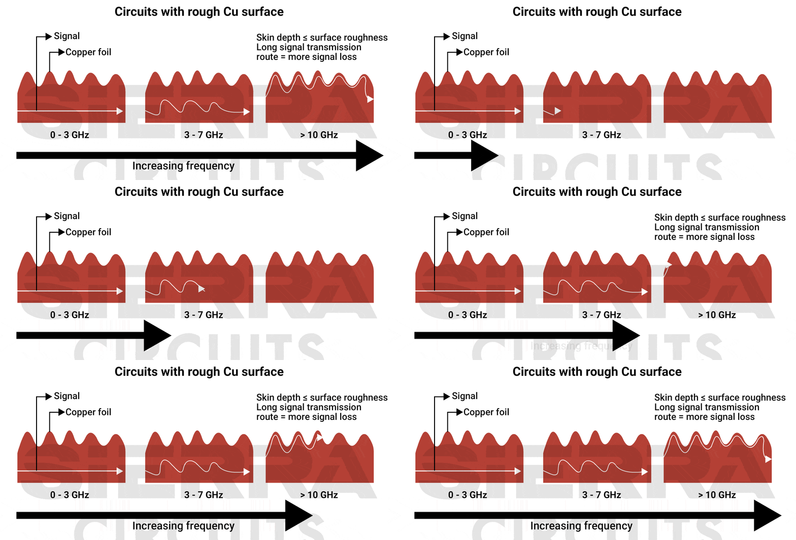
- Mitigate skin effect issues in microwave circuits by optimizing trace geometry, managing undercut during fabrication, and specifying precise sidewall plating conditions in your fab notes.
- Opt for electroless nickel plating or dip gold plating instead of HASL-lead free to reduce the odd effects of skin effect on high-frequency currents. Further, the highly solderable coating requires fewer leads, reducing environmental pollution.
- Utilize differential circuit topology to enhance immunity to crosstalk. Ensure optimum separation (3W) between differential signal pairs and other PCB traces.
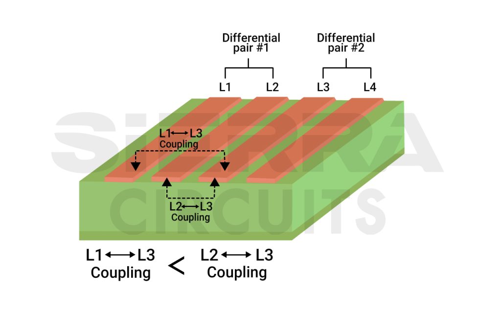
Two parallel differential pairs introducing crosstalk - Implement a low-impedance guard transmission line or circuit trace between two parallel transmission lines to mitigate crosstalk.
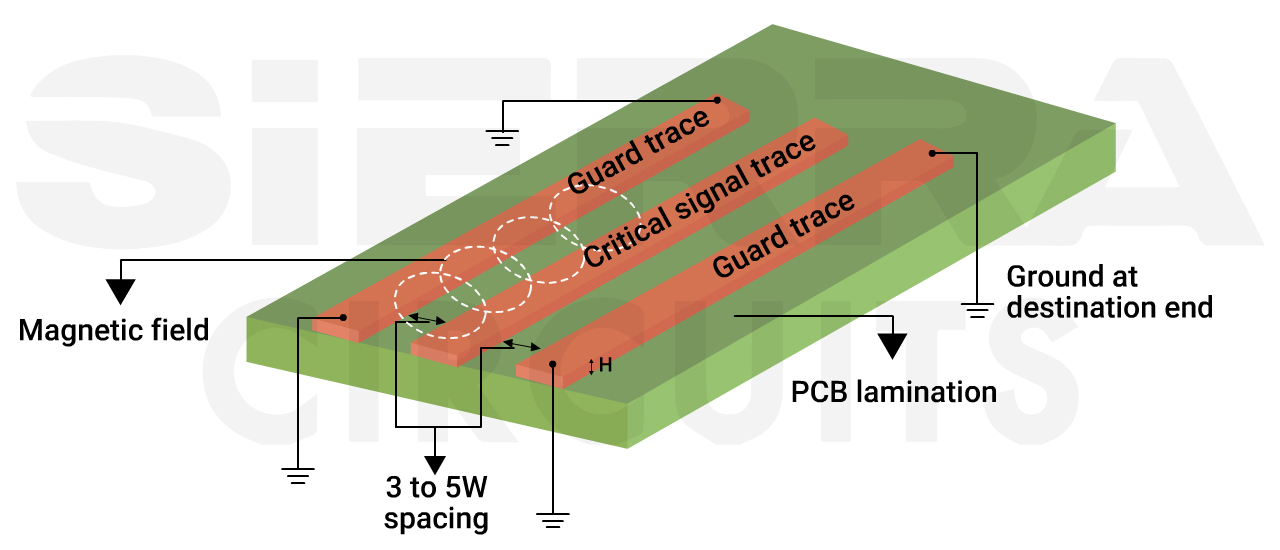
Guard traces protect critical signal traces. - Isolate analog and digital circuits to avoid interference. However, this may potentially reduce the efficiency of PCB area utilization.
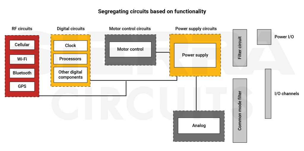
Segregating circuits based on their functionalities in microwave PCB design - Incorporate decoupling capacitors in power-supply filtering to reduce crosstalk through the power-supply lines.
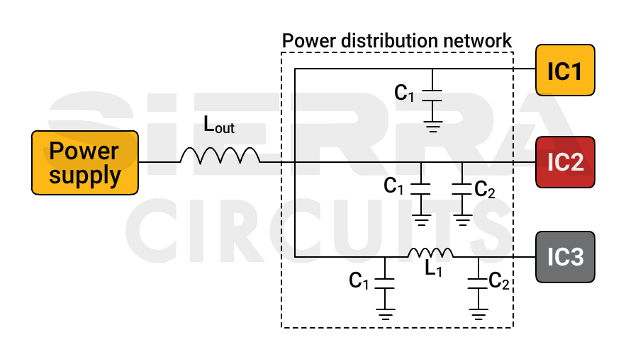
Crosstalk from signal sources like local and clock oscillators can affect power supply circuitry. This noise can propagate throughout the system, coupling into the inputs of sensitive components like amplifiers. As a result, the amplifier may inadvertently amplify these unwanted signals, causing distortion and reducing signal integrity.
- Consider higher-layer count stack-ups for greater routing flexibility in complex designs. However, they result in a thicker PCB and potentially higher costs. Determine the optimal layer count based on specific design requirements. A range of 6 to 12 layers is common for RF PCBs, offering a good balance.
As the layer count increases, the risk of layer misalignment during fabrication also rises. This misalignment can result in impedance mismatches and signal integrity issues.
To tackle this, at Sierra Circuits, we control curing parameters like temperature, pressure, and time to minimize inherent and residual stress.
Thus eliminating the risk of layer misalignment and delamination.
See RF and microwave PCB capabilities to learn more.
3. Shorter wavelengths make the board more susceptible to EMI
Electromagnetic interference includes both conducted currents and radiated electromagnetic fields. Many EMI issues arise from grounding problems, often beginning with the PCB stack-up.
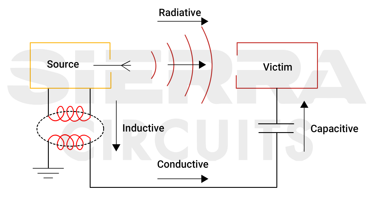
Microwave circuits operate at much higher frequencies, where the effects of EMI become more significant. At these frequencies, the wavelength is shorter, making circuits more susceptible to interference from nearby electromagnetic sources. Addressing these issues is crucial to overcoming key microwave PCB design challenges.
Board-level shielding (BLS) can be designed as a protective barrier around sensitive components or circuits. This method restricts the propagation of electromagnetic energy between sources and receptors to acceptable levels. BLS can be manufactured in various sizes, shapes, and heights.
For more high-speed PCB design tips, download our eBook.

High-Speed PCB Design Guide
8 Chapters - 115 Pages - 150 Minute ReadWhat's Inside:
- Explanations of signal integrity issues
- Understanding transmission lines and controlled impedance
- Selection process of high-speed PCB materials
- High-speed layout guidelines
Download Now
6 factors to consider when designing board-level shielding
- Shielding performance can be influenced by the source’s frequency and position, field configuration, and distributed inductances and capacitances when the shield is positioned within the near-field of the source. It should be approached as a coupling problem rather than a radiation issue.
- Key factors to evaluate include the coupling between the source and shield, mutual coupling among elements, shield termination effects, and grounding techniques. Additionally, consider the diffusion of currents through the shield and the impact of bends and corners, which can create external voltages.
- The effectiveness of board-level shielding depends on the PCB’s design around the mounting area. To enhance shielding performance, ensure that traces are adequately spaced, position vias away from the shielded region, and minimize the number of holes near the shielded area.
- With increasing frequencies, devices generate more heat. Ensure proper thermal management using thermal pads and heat sinks to maintain performance and reliability.
- Consider resonance effects at higher frequencies, as structures can self-resonate. Even minimal coupling at these elevated frequencies can lead to strong oscillations that may propagate to other points within the enclosure.
- At higher frequencies and shorter wavelengths, it’s important to consider the size and number of holes in a shield, as well as thermal effects. However, these concerns are less significant due to the near-field effect, where capacitive and inductive coupling have a greater impact on shielding effectiveness than aperture size.
7 strategies to tackle EMI challenges in microwave PCB design
- Implement a dedicated ground plane for each RF layer to maintain a consistent ground potential throughout the system, effectively reducing EMI in your PCBs.
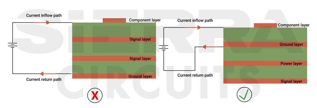
Desired ground plane placement in RF PCB designs. - Arrange signal traces on different layers of multilayer PCBs in orthogonal orientations (e.g., horizontal on one layer and vertical on another) to minimize electromagnetic coupling and interference between layers.
- Use high-performance insulated circuit boards with stable dielectric constants to efficiently manage electromagnetic fields between insulating materials and adjacent wiring.
- Design solid power and ground planes in your stack-up. These layers serve as protection to reduce EMI and offer consistent voltage references. Power and ground planes are placed as adjacent internal layers.
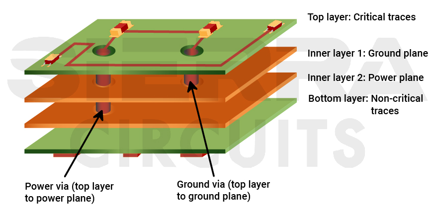
Ensure a solid reference plane to reduce EMI in your PCB. - Employ solder dams instead of covering the entire surface of the board with solder resist material. This approach mitigates significant changes in electromagnetic energy within microstrip designs, addressing uncertainties in the thickness and insulation properties of the solder resist.
- Opt for surface-mount components over leaded components in high-frequency environments to avoid the adverse effects of protruding leads and tapped inductors. These protruding leads create unwanted inductance, which may increase electromagnetic interference and radiation, particularly at high frequencies.
- Use gaskets to maintain shielding effectiveness by treating seams to prevent RF leakage. Gaskets create conductive contact across mating surfaces, ensuring continuous seams between metal pieces. Further, it reduces the need for closely spaced fasteners (about 25mm or 1 inch apart).
In compression configurations under a flat cover panel, gaskets use pressure to keep the seam shielded. In shear applications, a flange or channel arrangement preserves shielding without sliding.
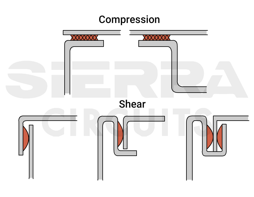
Select gaskets based on shielding needs, environment, and space; both beryllium copper (BeCu) and metalized fabric gaskets ensure EMI compliance:
-
- BeCu gaskets: Offer the highest attenuation over the widest frequency range for both compression and shear applications. They feature a solid finger design for high conductivity, a large contact area, low inductance, and a wiping action to remove oxide buildup. They resist over-compression, though slots between fingers permit RF energy at high frequencies.
- Metalized fabric gaskets: Made of conductive fabric over a foam layer. These gaskets offer high attenuation, determined by the level and matrix of conductive particles and compression force. They come in various shapes (rectangular, square, D-shaped, bell-shaped, knife-shaped, etc.) to accommodate different compression ranges, including low values.
To mitigate design challenges in RF boards, see 9 factors that impact RF PCB designs and tips to resolve them.
Key takeaways:
- Ensure trace widths are consistent to prevent impedance mismatches and facilitate maximum power transfer by matching the characteristic impedance (50Ω).
- Address skin effect losses by maintaining trace thickness below 0.1 times the material’s skin depth to minimize energy conversion to heat.
- Apply guard traces between critical signal lines to reduce crosstalk, addressing one of the key microwave PCB design challenges.
- Avoid unintentional stubs on RF traces to minimize circuit attenuation and signal degradation.
- Prevent signal reflection by terminating transmission lines with loads matching the characteristic impedance.
- Keep signal traces shorter than 1/20 of the wavelength to reduce signal loss and improve impedance control.
- Isolate power and ground layers in inner PCB layers to shield and reduce signal trace lengths, minimizing cross-interference.
- Implement ground planes to maintain consistent ground potential and reduce EMI reception issues.
- Arrange signal traces on different layers of multilayer PCBs in orthogonal orientations to minimize electromagnetic coupling.
- Use gaskets (BeCu or metalized fabric gaskets) to prevent RF leakage and maintain shielding integrity.
Microwave PCB layout design presents numerous challenges, primarily due to the unique behaviors of high-frequency signals. Maintaining consistent impedance, utilizing proper trace lengths, controlling crosstalk through strategic spacing and shielding, and employing advanced grounding techniques can significantly mitigate these challenges.
Need help designing a microwave circuit board? Post your questions on our PCB forum, SierraConnect. Our design experts will resolve them.
About Pooja Mitra : Pooja Mitra is an electronics and communication engineer. With an experience of over three years in the PCB industry, she creates industry-focused articles that help electrical and PCB layout engineers.







What’s your go-to method for impedance tuning when dealing with irregular trace geometries?
Which types of shielding techniques do you find most effective for GHz frequency layouts?
The preferred method for impedance tuning with irregular trace geometries involves using a vector network analyzer (VNA). By setting up a Smith chart or polar display, traces are adjusted to achieve optimal return loss.
For GHz frequency layouts, the most effective shielding technique is the use of a Faraday cage. Leader Technologies offers a variety of small, semi-custom shielding solutions, some of which can be trimmed to fit specific requirements.