Contents

On-demand webinar
How Good is My Shield? An Introduction to Transfer Impedance and Shielding Effectiveness
by Karen Burnham
Electromagnetic interference, or EMI, is a major cause of signal integrity problems for PCBs. All circuits generate EMI and get affected by it.
It may be caused by unexpected radiated emissions as well as through interference conducted along with cables and traces. Common reasons for high EMI in circuit boards include poor grounding, lack of shielding, and poor circuit design. Methods to control EMI include the elimination, attenuation, and control of emissions at their source.
EMI is coupled to other circuits through radiation or conduction. In both instances, the degree of coupling and the magnitude of the EMI increases with frequency.
EMI requirements
International EMI standards specify the acceptable levels of emissions. Class A devices that are intended for business use have slightly lower, more relaxed limits than class B devices, intended for domestic use. Class B limits are around 25 % more rigid than those for class A. The two main bodies controlling EMI Standards are the FCC and the European CISPR. Although these standards are similar in many ways, the CISPR requirements are slightly tighter.
Refer to the following tables to know the EMI limit according to the classes.
| FCC class A | ||
|---|---|---|
| Frequency of Emission (MHz) | Quasi-peak Limit (dBμV) | Average Limit (dBμV) |
| 0.15 - 0.50 | 79 | 66 |
| 0.50- 30.0 | 73 | 60 |
| FCC class B | ||
|---|---|---|
| Frequency of Emission (MHz) | Quasi-peak Limit (dBμV) | Average Limit (dBμV) |
| 0.15 - 0.50 | 66 to 56* | 56 to 46* |
| 0.50- 5.00 | 56 | 46 |
| 5.00- 30.0 | 60 | 50 |
Although this article is primarily about EMI susceptibility, for electromagnetic compatibility to exist, products should be immune to generally acceptable levels of EMI and should not generate EMI that exceeds the levels specified in the standards. Make sure to limit excessive radiation from entering or exiting the board at the entrance point.

High-Speed PCB Design Guide
8 Chapters - 115 Pages - 150 Minute ReadWhat's Inside:
- Explanations of signal integrity issues
- Understanding transmission lines and controlled impedance
- Selection process of high-speed PCB materials
- High-speed layout guidelines
Download Now
EMI sources
It can originate from external or internal sources and can be conducted over cables, connectors, and traces. EMI problems are caused by noise, antennas, and pathways to radiators. Electromagnetic interference is commonly generated from the following:
- Transformation of differential signal to a common signal that goes on external-twisted pair cable.
- Ground bounce that creates common currents on external single-ended shielded cables.
EMI sources include:
High-frequency signals: These signals are more prone to excessive radiation, especially if proper shielding is not done. At high frequencies, the inductive effect of a trace or line increases, and as a signal is transmitted, its magnetic field couples the signal to adjacent lines. The effects are aggravated by higher frequencies associated with fast signal rise time.
Signal harmonics: Square wave signals contain odd harmonics, particularly the third, fifth, seventh, and ninth harmonics.
Transients: External conducted and radiated transients exacerbate EMI. Sources include lightning, circuit breaker switching, power-switching devices, power converters, and disturbances on power and communication lines.
Internal EMI sources: Fast signal transitions are strong EMI emitters. These include high-frequency clock signals, high-speed data lines, and large di/dt variations due to the switching of high-speed logic circuits.
Impedance mismatching: High-frequency signals in PCB circuits exhibit transmission line characteristics, and reflection and ringing occur if the receiver and transmitter impedances don’t match the characteristic impedance of the trace.

How is EMI coupled
EMI coupling mechanisms describe how it travels between the source and receiver (affected devices). It is crucial to understand the nature of electromagnetic interference and the way it is being transmitted from the source to the receiver to fix the problem. Four kinds of EMI coupling are used to connect a source with a receiver: conduction, radiation, capacitive and inductive coupling. Next, we’ll look at the coupling mechanisms individually.
Conduction
This occurs when the interfering signal travels along with input cables or connecting wires. Coupling frequencies are generally less than 30 MHz. Any line entering or leaving a board is susceptible to coupling radiation. Interconnecting cables between two sources are a good source of EMI transferring one path to the other side of the board. As such, long cables help control EMI. These types of EMI are common on the power supply lines and are heavily concentrated on the H-field component. On power lines, interference can appear either as common mode conduction (on the +ve and -ve lines or tx and rx lines) or as differential mode conduction. A method for mitigating conduction coupled interference is to use filters and shielding over cables.
Radiation
EMI radiation occurs primarily at frequencies above 30 MHz. Internally, EMI can be radiated by the electric field generated by a fast transient signal that utilizes a stub or loop as an antenna. EMI can also be inductively coupled. Traces without a return path will generate common-mode radiation and those with a return path produce differential mode radiation. The radiation far-field strength is directly related to frequency in single-ended circuits and the square of the frequency for differential signal circuits. Contrary to conduction, it involves no physical connection between the source and receiver since the interference is emitted (radiated) through space to the receiver.
Capacitive coupling
This happens between two connected devices. Capacitive coupling occurs when alternating electrical signals are transferred from one segment of a circuit to another via stray/parasitic capacitances.
Inductive coupling
EMI occurs when a conductor induces interference in another conductor nearby based on electromagnetic induction.
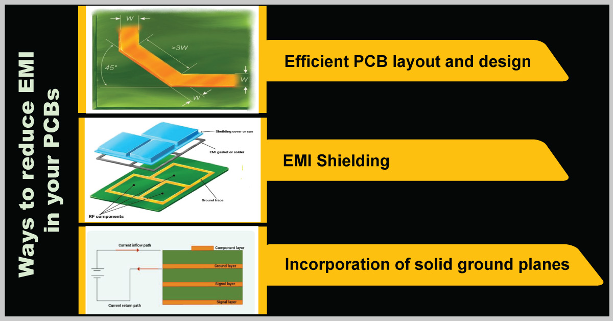
Designing circuits to minimize EMI
Techniques to minimize EMI include the control, attenuation, and elimination of emissions at the source as well as designing for clean and smooth transitions that are precisely placed in time. Here are several ways this can be achieved:
Good PCB layout and design
- Keep trace lengths short and away from the edge of the board.
- Avoid layer changes (especially where signal paths are concerned), and don’t route high-speed signals over slots.
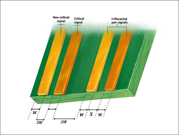
- Reduce inductive effects by employing three-terminal capacitors, keeping differential traces close, and placing other traces at least three trace widths apart.
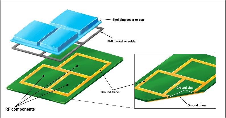
EMI shielding
- Shielding prevents electromagnetic interference from entering the board’s circuitry. It is possible to encase a specific component that generates EMI by wrapping it in a component shield – reducing the size of the antenna loop and blocking EMI. The shield may enclose the entire board to protect against EMI from outside sources.
- Cables that are carrying analog and digital signals create issues. These issues result in parasitic capacitance and inductance. Cable shielding avoids EMI.
Component layout
- Isolate sensitive components: Assign different board areas for diverse circuits keeping oscillator circuits away from other components. Keep high-speed components away from disturbing signals and I/O connections.
- Choose logic families carefully: Select logic families that have a high noise margin and avoid high-speed logic.
- Loop Area: To avoid excessive amounts of EMI, make the loop area as minimal as possible.
- It is always a good idea to separate analog and digital circuits. The proximity of these components can result in crosstalk.
- It is also important to keep high-speed signals close to the ground plane.
Auto-group the recurring circuit blocks to speed up the routing process.
These measures help maintain acceptable levels of crosstalk, noise, and radiation.
Ground plane
- Pay careful attention to grounding: Use a large, unbroken ground reference plane and connect ground islands to the ground plane using numerous vias. Ensure that return paths in the ground plane are not crossed.
- Make the ground area as large as possible. A larger area allows signals to disperse more evenly, reducing emissions, crosstalk, and noise.
- Solid ground planes: These planes are ideal for multi-layer boards. Solid ground planes, on the other hand, offer lower impedance levels.
- Each component should be connected to a point on a ground plane.
See our interview with Rick Hartley on how grounding controls emi and noise in pcb.

Controlled Impedance Design Guide
6 Chapters - 56 Pages - 60 Minute ReadWhat's Inside:
- Understanding why controlled impedance is necessary
- Stack-up design guidelines
- How to design for impedance
- Common mistakes to avoid
Download Now
Few additional considerations
- Apply transmission line design: Design PCB layers and trace widths to provide the right line impedance, and match the source and receiver impedances to the trace impedance using terminating resistors. As a guideline, transmission line theory should be applied to any line length in inches that exceeds the signal rise time in nanoseconds. Although metal traces are resistive at low frequencies, they are largely inductive at high frequencies.
Also read: Unlock Your Signal Integrity Analysis Potential

- EMI Propagation: This won’t affect DC or lower frequency signals or components, only higher frequency signals and high impedance.
- Avoid antennas: Unconnected stubs and traces without return paths act as antennas as do ground and power loops.
Electromagnetic interference affects PCB design in two ways, through generation and susceptibility. Although the focus has been on reducing the effect of internal and external EMI within boards, these techniques are equally effective in reducing emissions. Limiting the deleterious effects of EMI significantly improves signal integrity on boards. Please let us know in the comment section if you have any questions about EMI and signal integrity.
Also see, how to mitigate EMI issues in your PCB designs by Daniel Beeker.