Related Categories — Manufacturing » PCB Assembly
PCB Design for Assembly Checklist: 9 Important Checks for Layout Engineers
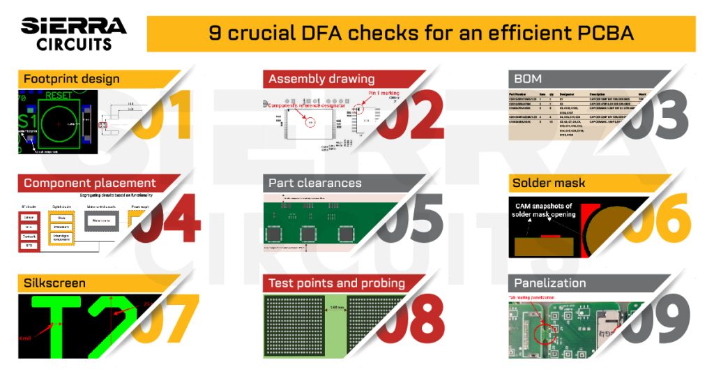
Here’s a PCB design for assembly checklist you can refer to before you proceed with the assembly process. This includes […]
PCB Assembly
IPC-6012 or IPC-A-600: Which Standard Should You Use?
The association connecting electronics industries – commonly known as IPC – is an international trade association serving the ... more »
IPC
Why Do PCBs Cost Less in China Than in the USA?
PCB manufacturing costs are typically lower in China than in the USA due to reduced labor expenses and ... more »
PCB Manufacturing
PCB Design for Assembly Checklist: 9 Important Checks for Layout Engineers
Here’s a PCB design for assembly checklist you can refer to before you proceed with the assembly process. ... more »
PCB Assembly
IPC-6012 or IPC-A-600: Which Standard Should You Use?
The association connecting electronics industries – commonly known as IPC – is an international trade association serving the ... more »
IPC
Why Do PCBs Cost Less in China Than in the USA?
PCB manufacturing costs are typically lower in China than in the USA due to reduced labor expenses and ... more »
PCB Manufacturing
PCB Procurement Checklist for Hardware Engineers
When procuring PCBs, engineering and sourcing teams should follow a structured checklist that validates BOM accuracy and assesses ... more »
Manufacturing
How to Design an HDI PCB Stack-up
When designing an HDI PCB stack-up, you need to choose the right build-up architecture and define a via ... more »
HDI / Blind & Buried Vias
How to Select and Place RF Components for PCB Designs
Choosing the right RF PCB components and placing them appropriately helps you avoid critical issues such as insertion ... more »
PCB Assembly
What Are QFN Packages?
The surface-mount IC packages that are assembled on a PCB are available in different types. The most popular ... more »
PCB Assembly
How to Design Reliable Microvias in Your PCBs
Key design strategies for enhancing microvia reliability include selecting suitable materials for laser drilling, adhering to IPC-T-50M guidelines, ... more »
HDI / Blind & Buried Vias
How to Pick the Right Flex PCB Materials for Your Application?
When selecting flex PCB materials, you need to consider the application type (dynamic or static), stiffener requirements, and ... more »
Flex PCBs
Fabrication, Procurement, & Assembly. PCBs fully assembled in as fast as 5 days.
- Bundled together in an entirely-online process
- Reviewed and tested by Engineers
- DFA & DFM Checks on every order
- Shipped from Silicon Valley in as fast as 5 days
Fabrication. Procurement & Assembly optional. Flexible and transparent for advanced creators.
- Rigid PCBs, built to IPC-6012 Class 2 Specs
- 2 mil (0.002″) trace / space
- DFM Checks on every order
- 24-hour turn-times available
Complex technology, with a dedicated CAM Engineer. Stack-up assistance included.
- Complex PCB requirements
- Mil-Spec & Class 3 with HDI Features
- Blind & Buried Vias
- Flex & Rigid-Flex boards


