


Contents

On-demand webinar
How Good is My Shield? An Introduction to Transfer Impedance and Shielding Effectiveness
by Karen Burnham
When placing components in KiCad, you must follow a structured approach to ensure efficiency in your PCB design. In this KiCad tutorial, you’ll learn how to import a schematic, define board dimensions, set up a stack-up, and organize critical components.
10 things to check before placing components on your PCB layout
Before placing components in KiCad, ensure the following:
- Verify all components, connections, and labels are accurate in the schematic.
- Ensure you have access to the necessary component libraries.
- Assign correct footprints to all components based on their physical dimensions and specifications.
- Set design rules (e.g., clearances, trace widths) based on manufacturing and electrical requirements.
- Identify and plan the placement of critical components (e.g., power, connectors, high-speed components).
- Generate and import the netlist into the PCB layout to establish connections between components.
- Plan your stack-up. Decide the required layers and estimate the ground and signal planes required.
- Consider ground and power distribution networks, including decoupling capacitors.
- Make sure the PCB dimensions and shape align with your design constraints.
- Identify high-speed or sensitive signal paths and plan for optimized routing.
For more tips on high-speed design, read how to create a schematic for high-speed designs in KiCad.
Placing components efficiently in KiCad
Step 1: Open the layout file
Before placing the component, ensure your KiCad project has a schematic ready for conversion to a PCB layout.
When you create a KiCad project, the software will automatically create a default layout file. You can import the schematic into this file.

To learn how to create a schematic and symbol library, see creating a schematic and symbol library in KiCad.
Step 2: Import your schematic into the PCB layout
Next, you must translate your schematic into a layout with effective component arrangement.
Click Update PCB from Schematic under Tools. This option in KiCad synchronizes your PCB layout with changes made in the schematic. It imports the netlist, adds new components, removes redundant components, and updates connections.
This eliminates the need to manually export the netlist from the schematic editor and importing to the layout editor.

Check all the below options in the Update PCB from Schematic dialog:
- Re-link footprints…: Ensures that components in the PCB layout are linked to their respective footprints.
- Delete footprints with no symbols: Removes any footprints not present in the schematic.
- Replace footprints…: Updates footprints if changes were made in the schematic.
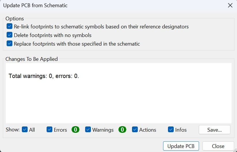
Update PCB from the Schematic option in KiCad.

Next, ensure that all components have been imported correctly. Address any warnings or errors that may have appeared during the import process.
Click Update PCB to complete the import of the designed schematic.

For step-by-step guidelines on designing a PCB in KiCad, download our eBook.

KiCad Design Guide
10 Chapters - 161 Pages - 180 Minute ReadWhat's Inside:
- Creating a component symbol library
- Setting up board parameters and rules
- How to route differential pairs
- How to place of components
Download Now
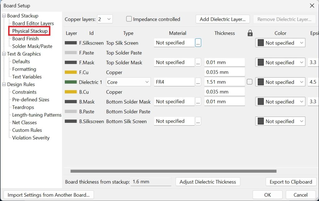
Step 3: Define board stack-up in Pcbnew
Before placing components, you must define the board’s physical dimensions and layer stack-up. This setup ensures that your board has the correct size and layer configuration.

- Open Board Setup.
- Under Board Editor Layers, define the layers.
Click OK to save your settings.

- Under Physical Stackup, choose the number of copper layers (up to 32) and configure the thickness and material details.

Step 4: Draw the board outline
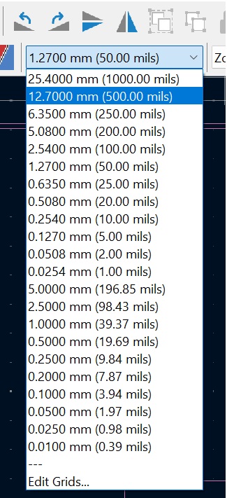
Before drawing the board outline, configure the grid settings. We have set the grid size to 500 mil for better precision.
Configuring grid settings before drawing the layout. To draw the outline, select Edge.Cuts in the Appearance panel on the right-hand side. Use the Draw Line tool to define the corners and edges of your PCB. Complete the outline and ensure it is closed and matches your design specifications.

Step 5: Set the Grid and Drill/Place File origin
To place the grid origin, go to Place, select Grid Origin and click at the bottom-left corner of your board outline. For adding drill/place origin, select Drill/Place File Origin and place it on the bottom-left corner of the outline.

Grid origin: It is a reference point on the PCB where the coordinate system starts (0,0). It determines the base location from which all component and trace placement measurements are referenced.
Adjusting the grid origin is helpful for precise alignment and for working with relative coordinates during the PCB design process.
Drill/place file origin: It is the reference point used when generating drill and placement files for manufacturing. It defines the starting coordinates from which the locations of component placements and drill holes (via, pad holes) are measured.
Setting the correct drill/place file origin is essential for aligning your design with the manufacturing equipment and ensuring the board is fabricated correctly.
Step 6: Add mounting holes to the board outline

Follow these steps to add mounting holes on your board:
- Change the grid settings to 50 mil. This provides finer precision for placing small components.
- Drag the mounting holes and place them at the four corners of the board outline.
- Ensure there is sufficient space around mounting holes to prevent issues during assembly.
- Keep a minimum of 25 mil board edge to mounting hole clearance.
- Use the origin as the reference point to calculate dimensions.
- Lock the mounting holes. For this, select all four holes, right-click, and choose Lock under Locking. This will prevent accidental movement.
- Verify if the holes are locked by checking the object panel.

Step 7: Arrange connectors and key components
- Begin component placement with major connectors like USB ports, power jacks, and other critical components.
- Turn on the Footprint Text in the Objects tab on the right-hand side panel to identify and place components correctly.

- Plan and place the connectors at the board’s edge according to their specifications. For instance, here, the USB connector is a right-angle connector. It has a marking that needs to coincide with the board edge.
- Place the connector accurately. Change the grid setting for a clearer view.
- You can check the component placement in KiCad by using 3D visualization. For this, go to View and select 3D Viewer. Ensure you have placed the components in the right position.

Download our eBook for step-by-step guidance on creating custom libraries and linking symbols to footprints in KiCad 9.

KiCad 9 Step-by-Step Guide
6 Chapters - 41 Pages - 30 Minute ReadWhat's Inside:
- A complete KiCad 9 workflow from project creation to production file generation
- Step-by-step guidance on creating custom libraries and linking symbols to footprints
- Practical design checks: ERC and DRC
- Best practices for generating a clean BOM and fabrication-ready Gerber files
Download Now
Step 8: Place components based on functionality
- Arrange components logically by placing them to minimize routing complexity.
- Isolate digital, power, and analog circuits to minimize interference.
- Position signal ICs and their associated components close together.
- Ensure that connectors align with their respective nets for efficient routing.
- Place the ICs and keep the connections as short as possible.
- Ensure there’s enough space for traces and critical components are not too close to the edges.
- Adjust components to simplify routing paths and minimize crisscrossing connections by rotating the components.

- Make sure the connectors and other component courtyards are not overlapped.
- Refer to the schematic regularly to minimize errors.
- To facilitate the routing process, you can start to fan out the components at this stage. You also can avoid making adjustments to component placement for adding new vias in the later stage.

- Use the bottom side of the board for component placement for an easier routing process. Here, the comparator IC is placed backside of the regulatory IC for efficient placement.

KiCad version 9 brings component population control at the sheet level, enabling you to manage DNP (do not populate) requirements directly within schematic sheets.
Step 9: Position decoupling capacitors and crystals
When designing a PCB in KiCad, placing capacitors and crystals is crucial for ensuring optimal circuit performance.

Arrange decoupling capacitors close to the IC power pins to minimize noise and improve power stability. It also reduces the inductive effects of the PCB traces, allowing the capacitor to filter out high-frequency noise effectively.
Always place the decoupling capacitor with the lower capacitance value closer to the power pin or output. In comparison, the capacitor with the higher capacitance value can be placed slightly farther away.
In the example below, the lower value capacitor is placed closer to the ground and voltage input pin.

This arrangement ensures that the lower-value capacitor can effectively filter out high-frequency noise while the higher-value capacitor handles lower-frequency noise and bulk energy storage.
Crystals, often used with microcontrollers or oscillators, also require careful placement. Crystals should be positioned close to the ICs they are paired with to minimize the trace length between them.
This proximity helps reduce potential signal degradation or noise, which can lead to timing errors. Additionally, use short and direct traces to connect the crystal to the IC, with minimal routing complexity, to avoid introducing parasitic capacitance.

For more part placement tips, see component placement guidelines for PCB design and assembly.
It’s also important to consider the grounding strategy. Connect capacitors and crystals to a solid ground plane to ensure a low-impedance path and reduce the risk of noise coupling to the circuit.
Need help in designing reliable PCBs? Our engineering team can help you with thermal management, stack-up design, and DFM analysis.
You can book a meeting with our experts or call us at +1 (800) 763-7503.

Standard component clearances for optimal performance
| Parameters | Clearances |
|---|---|
| Min. part-to-hole spacing | 50-100 mil for manual soldering. 8 mil for others. |
| Min. part-to-annular ring spacing | 50-100 mil for manual soldering. 7 mil for others. |
| Min. part-to-edge spacing | 125 mil for large components. 25 mil for small components. |
8 benefits of accurate component placement
- Improved signal integrity: Reduces noise, interference, and distortion, ensuring better performance, especially in high-speed circuits.
- Efficient power distribution: Offers shorter power and ground connections, minimizing voltage drops and power losses.
- Reduced trace lengths: Results in shorter traces, reducing parasitic capacitance and inductance.
- Easier routing: Simplifies PCB routing, leading to cleaner layouts with fewer crossovers and vias.
- Enhanced thermal management: By placing heat-generating components at the center of the board, you can provide better airflow and heat dissipation, improving system reliability.
- Minimized crosstalk and EMI: Proper spacing between components reduces electromagnetic interference (EMI) and crosstalk between signals.
- Cost efficiency: Efficient use of space can lead to smaller PCBs, reducing material costs and manufacturing complexity.
- Simplified assembly and testing: Simplifies assembly process, testing, and troubleshooting.
Following the steps outlined in this KiCad tutorial, you can import your schematic, set up your board, and effectively place components on your layout. You can use KiCad’s 3D Viewer to verify your design.
Have queries on PCB design? Post them on our forum, SierraConnect, and our experts will answer them.

About Sushmitha V : Sushmitha V has a master's degree in power electronics and has over four years of experience in the PCB industry. Her areas of interest include circuit board manufacturing, assembly, IPC standards, and DFM/DFA practices.


Start the discussion at sierraconnect.protoexpress.com