


Contents

On-demand webinar
How Good is My Shield? An Introduction to Transfer Impedance and Shielding Effectiveness
by Karen Burnham
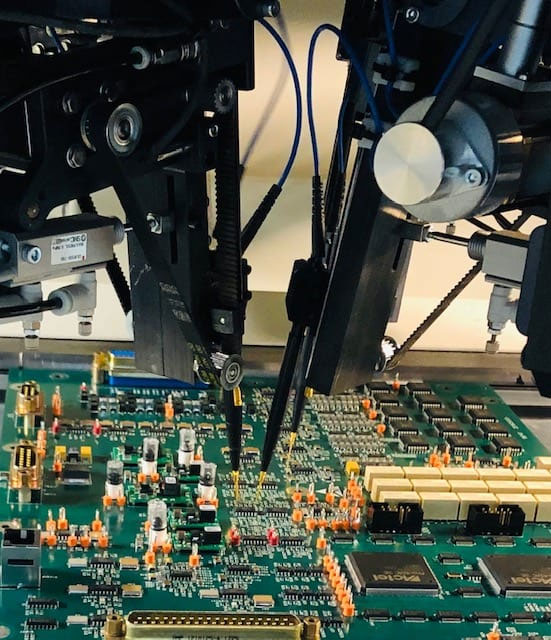
Mistakes occur while designing a circuit board. Performing a PCB design review will help you identify and rectify these errors. During this process, you must analyze and improve board elements such as stack-up, trace, vias, components, and others to ensure zero defects in the layout.
The DRC system can help you avoid some design flaws, but not all of them. Hence, having a final check will enable you to recognize unidentified faults. In this article, we will discuss the review and clean-up process in detail.

How to review a PCB layout?
The evaluation procedure extends to multiple stages of the layout development process:
Before constructing the layout, verify schematic drawings and bill of material (BOM) for the number of netlists and their naming, footprint dimension, assignment of DNI components, polarity, etc.
After finalizing the design, visually compare the schematics and constructed circuits to identify any errors. Run a design rule check from the layer stack-up to the component placement. Subsequently, clean up the PCB layout to remove the identified errors.
Finally, check for missing data in the production files before sharing them with the fab house.
Stack-up plane design and arrangement
The arrangement of ground, signal, and power layers is essential to produce an accurately functioning circuit. Therefore, consider the following points for efficient propagation of the signals.
- Always incorporate a solid ground layer in the build-up
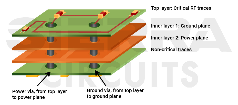
- Make sure you connect all the ground points to this plane through vias.
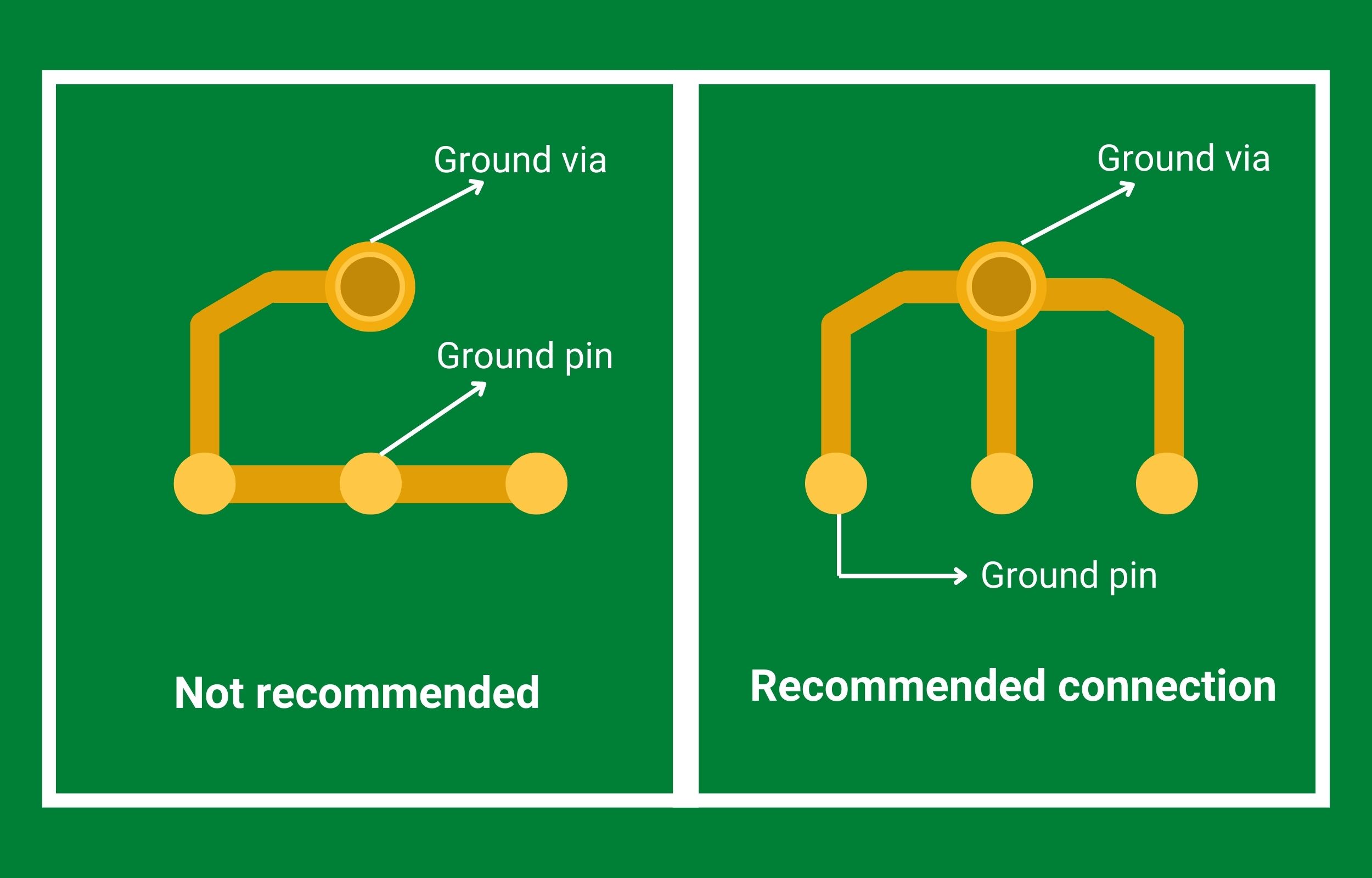
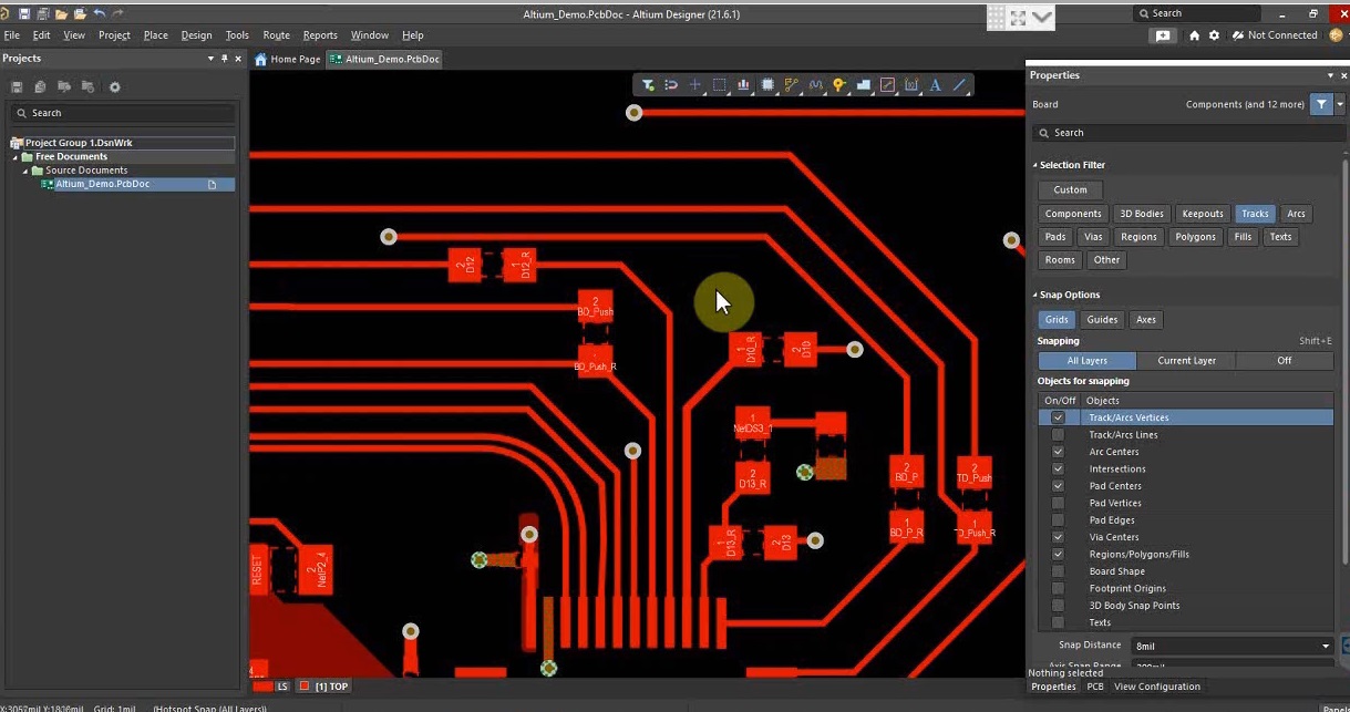
- It’s ideal to have separate via for every ground and voltage pin. However, if this is impossible, check if you have individually connected them to the hole, as shown in the image below.
- Avoid placing signal layers adjacent to each other.
- There should be symmetry in the stack-up arrangement to avoid warping.
- Remove the unwanted layers that design tools usually add.

Board dimension checks
- If you plan to install the circuit board in a casing, ensure its dimensions meet all the requirements.
- Check for optimum clearance, at least 10 mils, between the copper trace and the board edge.
- All non-plated holes, including mounting holes (minimum hole diameter of 3.3 mm), should have anti-pads. Additionally, the screw head/nut size should be greater than the diameter of the hole.
Placing polygons structures
Polygons (copper pours) are the areas around the components or traces filled with copper. They are created only on signal layers.
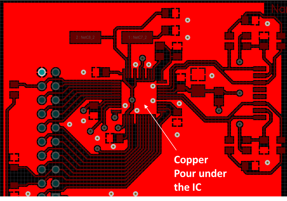
Ensure no floating copper pours are present in the layout while performing the PCB design review. If they are present, connect them to the ground plane. Furthermore, make sure that they do not create any open nets. If needed, place polygons in other layers to balance the copper distribution in the stack-up.
Reviewing trace placement in the board design
- Calculate the impedance and current carrying capacity of the trace and optimize their width accordingly.
- The length of the signal line and return path should be minimal to reduce noise and improve signal integrity.
- Ensure no open nets are in the circuit. If you want to keep an unconnected line, its length should be as short as possible.
- Maintain sufficient clearance between the traces to suppress crosstalk. Based on the copper weight, the optimum spacing is mentioned in the below table:
| Copper weight | Outer layer trace spacing (in mils) | Inner layer trace spacing (in mils) |
|---|---|---|
| 5 microns | 3 | 2 |
| 9 microns | 3 | 2.5 |
| 1 oz | 6 | 4.25 |
| 2 oz | 8 | 6.25 |
| 3 oz | 12 | 8 |
| 4 oz | 14 | 10 |
- Prevent sharp 90° bends, which can cause reflection and distort the signal.
- Make sure that there are no loops in the power and ground net.

High-Speed PCB Design Guide
8 Chapters - 115 Pages - 150 Minute ReadWhat's Inside:
- Explanations of signal integrity issues
- Understanding transmission lines and controlled impedance
- Selection process of high-speed PCB materials
- High-speed layout guidelines
Download Now
Via size and placement guidelines
Drilling a smaller hole is an expensive and time-consuming process. Hence, reduce the via size only if needed and try to keep the size consistent across the board. During the layout design review process, check the following parameters for the drilling:
- All the drill values are as per the requirement and verify that they are whole numbers.
- You have updated vias, plated, and non-plated hole names in the drill chart.
- The pad size is sufficient and completely covers the hole diameter.
- There should be a minimum clearance of 6 mils between two adjacent vias.
- Check if all the tolerances values are specified as per the following table
| Feature | Tolerance |
|---|---|
| Plated holes | ±3 mils |
| Non-plated holes | ±2 mils |
| Via | Typically ±2 mils (depends on drill and pad size) |
Solder mask openings and clearance
- Check if you have provided all the required openings in the solder mask layer while reviewing the PCB design.
- Make sure that via or components are not tightly spaced, to avoid sliver.
- Examine to see if you have provided sufficient solder dam, minimum 5 mils, in your design.

Complete and legible silkscreen
During the layout clean-up, ensure that the silkscreen layer is legible and the words/numbers/symbols do not overlap. We recommend using a minimum of 25 mil text height and 4 mil line width. You should also move the print if it is on the pads and holes. The legend should contain all the required information, such as:
- Product info: company logo, copyright notice, warning/hazard label(s), etc.
- Component details: name, orientation, terminal symbols, and IC pin one mark.
- Surface elements: mark LEDs, chips, mounting holes, fuse, etc.
- Board details: name, print date, and revision number.

Component placement and clearance
- Check the components’ orientation and clearance to make sure they do not overlap.
- Traces should not run under or between sensitive elements such as QFP/QFN, POP, or BGA.
- You can generate 3D files/ models to validate part placement.
- The bypass capacitors should be close to the IC power pin to reduce the effect of current spikes during the switching process.
- You should not place small components too close to high heat dissipating components like motor drives, amplifiers, transformers, and linear regulators. Provide a sufficient copper area for heat sinking.
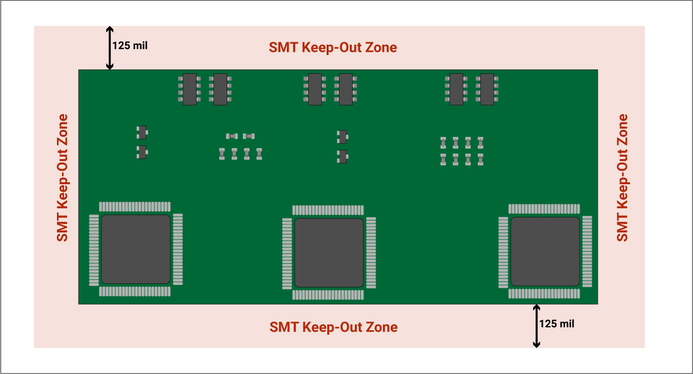
- There should be enough clearance between part to the edge of the board, minimum 125 mils.
Design review for PCB testing
You need to choose the testing method as per your board layout and provide test pins, accordingly. However, installing the test points may not be convenient, especially on a high-density board. Install them in such a way that they do not interfere with the actual circuit. For instance, a test pin should not become a stub or create an impedance mismatch in the high-speed interconnections.
Verify if you have provided all the pins on the signal traces that need to be accessed. Some types of testing may require additional space on the side to clamp the board or fiducial marks for registration. Ensure you meet these requirements in your design. Additionally, keep all the test points on a single side (preferably on the bottom side) of the board and clearly mark them in the prototype.
Need help in designing reliable PCBs? Our engineering team can help you with thermal management, stack-up design, and DFM analysis.
You can book a meeting with our experts or call us at +1 (800) 763-7503.

PCB design review for good signal integrity
Impedance mismatch and other sources of electromagnetic interference cause signal distortion in the layout. Regulating these issues is essential for achieving a better performance circuit.
Impedance mismatch issues
Maintaining a uniform impedance across the board is crucial for signal integrity, especially in high-speed and high-density circuits. If there are any mismatched impedances, implement termination components to mitigate them. For example, include termination resistors along the lengthy and closely spaced traces.
As mentioned earlier, keep the trace short and optimally spaced. Make sure that differential pairs are tightly coupled, and their lengths are matched. Along with this, check if you have fanned out BGA properly.
Check for controlled impedance.
If you plan to achieve a targeted controlled impedance, configure trace length, width, and spacing, accordingly. Check if the line has a ground reference on the top and bottom layers. Ensure that you have updated the layer, trace, and ohms in the fabrication notes.
If you are planning to implement the CI through the dielectric, mention your material requirement (type and number of prepreg/core ) in the production data.

Controlled Impedance Design Guide
6 Chapters - 56 Pages - 60 Minute ReadWhat's Inside:
- Understanding why controlled impedance is necessary
- Stack-up design guidelines
- How to design for impedance
- Common mistakes to avoid
Download Now
Regulating other EMC/EMI issues
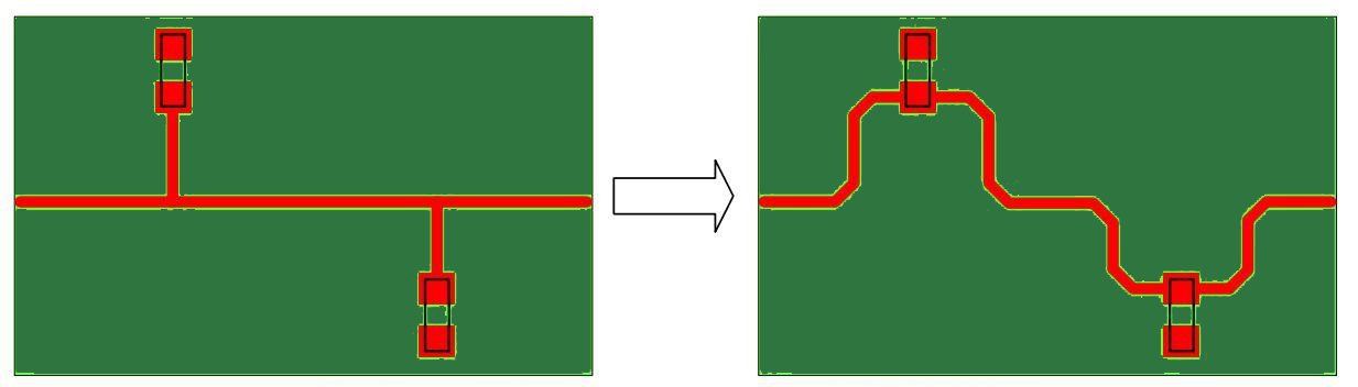
- As recommended earlier, check if there are any via stubs or unconnected nets that can act as an antenna and cause signal distortion. You can avoid them by implementing daisy chain routing, as shown in the image below.
- Every via will have its own capacitance and inductance effect, which can cause signal loss and reflection. Therefore, avoid placing vias on high-speed traces to prevent signal distortion.
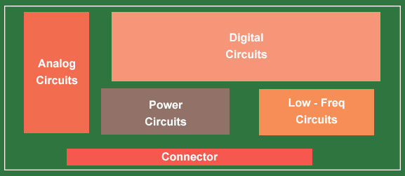
- Check if the analog and digital circuits are distinguished. Separate different kinds of traces (clock, audio, video) and segregate the components dealing with these signals. Include filters when there is communication between the groups. Also, confirm that you have implemented all the required decoupling capacitors to isolate AC and DC circuits.
Review of production files
After reviewing and cleaning up the board design, downloading the files and sending them for production may feel natural. But stop yourself from making this mistake. The data for board fabrication includes many documents, hence validated them carefully. Usually, the output files should consist of the following:
- Images of all the layers (Gerber)
- Solder mask layers (top and bottom)
- Silkscreen layers
- Bill of materials
- NC drill files for automated drilling equipment
- IPC netlist (number of nets present in the circuit)
- Master drawings
Validating the production data
Verify the below-mentioned data in the productions files before sending it for fabrication:
- Number of layers in the circuit
- Finished board thickness
- Material required according to the application
- Standards/classes with which the board has to comply
- Outer and inner layer copper thickness
- Color and type of solder mask finish (matt, semi-gloss, LPI)
- Color and type of silk screen
- Type of surface finish (HAL, gold, HAL lead-free)

- Controlled impedance requirement (specify the layer and the trace)
- Control dielectric (type and number of prepreg/core to use)
- Minimum trace width and spacing
- Number of drill holes in the circuit
- Types of via and their filling
Manufacturing tolerances are present in every stage of board fabrication and assembly. Maintaining a minimum tolerance depends on the manufacturer’s capability and process. Make sure to have a thorough discussion with your fabricator and alter your fab notes accordingly.
Updating the data after modifications
Modifications are inevitable while you are designing a board. Usually, there are many variations of the same layout, and updating the data in the exported files is crucial. Stay organized and include all the file revision dates. This will help you avoid mishaps and lower turn time.
To understand more benefits of good PCB design team collaboration, read how modular PCB design method simplifies complex layouts.

Yes, applying all the steps mentioned above may seem challenging. However, do not skip the reviewing process of the PCB layout. It is always better to do modifications in the designing stage rather than sending the board for rework. If you have any questions concerning the layout review and clean-up process, let us in the comment section. We will be happy to help you.

About Sushmitha V : Sushmitha V has a master's degree in power electronics and has over four years of experience in the PCB industry. Her areas of interest include circuit board manufacturing, assembly, IPC standards, and DFM/DFA practices.


