Contents
We were lucky enough to meet Heidi Barnes during DesignCon 2022. Keysight’s most famous Senior Applications Engineer discussed signal integrity and power integrity in high-frequency boards.
Heidi Barnes is a senior application engineer for high-speed digital applications in the design engineering software group of Keysight Technologies. Her interest lies in the application of electromagnetic, transient, and channel simulators to solve signal and power integrity challenges. Heidi is the author of over 20 papers on SI and PI, recipient of the DesignCon-2017 Engineer of the Year, and the prestigious NASA Silver Snoopy Award for her work on hydrogen fire and gas detection.
How do you utilize frequency and time-domain measurements and simulations to meet the recent power delivery demands?
Heidi Barnes: It is interesting to meet the new challenges of power delivery to high-speed digital loads with the power rails dropping to lower voltages, and the currents continuing to increase. I was talking with Steve Sandler earlier about customers out there with 1000 or 2000 amps products and it is amazing what is being done in the electronics industry today. We find it is happening fast in the power integrity world. We have talked a lot about target impedance looking at power delivery in the impedance domain. But I think one of the things that are happening rapidly right now is this interest within the industry to go between frequency and time domain, doing design and simulation in the frequency domain to optimize the impedance, going from your source of power, your voltage regulator module, your power supply, to your decoupling capacitors, to your load. You have to look at the impedance matching there, and what the whole system looks like in terms of the impedance versus frequency. But then you have to take that optimized PDN impedance and excite it with a time-domain signal and look at the voltage ripple on that power rail with that impedance design. We can go back and forth between impedance and frequency and realize the impedance domain is almost like TDR in the signal integrity world. As Eric Bogatin says, hack the back, hack the transmission line, or figure out where the discontinuities are, where the problems are. TDR is used in this SI world to look at, spatially, what’s going on in your transmission line delivery of your high-speed signal.
In the power world, if we look at impedance versus frequency, the low frequency is where your power supply is operating. The mid-range frequencies are where the decoupling capacitors are operating, and in the high frequencies, it is your package die capacitance. You can start to look at what part of your power delivery is having problems because the impedance versus frequency helps you debug a little bit. Whereas in the time domain, a lot of times, it’s much harder to see what part of the system is having trouble.

What are the best practices for power integrity designers to optimize the PDN in high-speed electronics?
Heidi Barnes: If you want to optimize a power delivery network, you need to look in the impedance domain. This includes what the impedance looks like from low frequency to high frequency from the DC operation of your power supply, where the power supply becomes inductive, and impedance increases, because it cannot keep up. The control loop is not fast enough to deliver a high-frequency power, and so that is why your decoupling capacitors have to take over. Essentially, in the impedance domain, you can see what is happening, that the power supply impedance starts to increase. You need to add capacitors onto your printed circuit board to provide that charge delivery at those higher frequencies, and to maintain the low impedance. Similarly, you have to keep adding decoupling capacitors until the capacitors and the package can take over, and that is at a much higher frequency, and that provides you some guidelines as to what your decoupling capacitors need to do.
I call it a misnomer a little bit. You are designing a power supply, the power supply works at a low frequency. Your PCB or application designer has to say that he is going to design the power in the mid-range, the decoupling capacitor is the power source for those frequency ranges. You see that when you look at the frequency domain.
To learn how we resolved component placement issues by sequentially placing power sources, see our case study, designing microcontroller and functional PCBs with an antenna.

High-Speed PCB Design Guide
8 Chapters - 115 Pages - 150 Minute ReadWhat's Inside:
- Explanations of signal integrity issues
- Understanding transmission lines and controlled impedance
- Selection process of high-speed PCB materials
- High-speed layout guidelines
Download Now
How do you select the right decoupling capacitors for achieving flat impedance?
Heidi Barnes: Decoupling capacitors sound easy. I need a capacitor with enough charge storage to cover a certain range or amount of charge delivery. But when you buy a capacitor, you get an inductor for free. You buy a capacitor at lower frequencies, it looks like a capacitor, and it is well behaved. But again, the capacitor has parasitic, and when you get up to a high enough frequency, it transitions to an inductor. They call that the self-resonant frequency where that transition happens.
At that point where it changes, you also see the pure resistance. As it is changing from a capacitor to an inductor, you also see the series resistance that is a part of the capacitor. So a capacitor gets an extra series resistance and a series inductance. The big problem in the industry is, how do I characterize those parasitic? When you measure a capacitor, you have to mount it on something, you have to fix it, and that will have some inductance in it. The mounting has inductance depending on how you do the pads on the board, and how the via topologies make that connection from the power to the ground. We call that mounting inductance or fixture inductance.
When the industry measures that capacitor, they don’t always tell you how much of that mounting inductance is still left in their vendor data. If you are doing a simple spice simulation with lumped models and you don’t have any circuit board parasitic, then you want some of that mounting inductance in your simulation because it is more realistic. But nowadays, when we have so many simulators, there are options for simulating a printed circuit board with the parasitic using an EM simulator for the PCB model. But that EM model includes the mounting inductance. It has the pads for the capacitor. It has the via topology and the power ground spacing and stuff. You already are calculating that mounting inductance. The problem is that the vendor model often includes it and you don’t want to double count.
We need to design that power delivery over bandwidth with our decoupling capacitors and the large capacitors will have a lot of inductance. Then I need a smaller capacitor with lower inductance. You keep going to smaller capacitors to get charge storage out to a higher frequency with less inductance. But if my model does not have the right inductance then it is very hard to optimize the design for a certain impedance. I grab a model and I’m double counting the inductance, then I am going to overdesign, add a lot more capacitors than I need to, and try to bring the inductance down. That is the biggest challenge of getting accurate models of those capacitors for use with an EM model.
To learn the crucial signal integrity elements required to achieve a flawless PCB design, see how to achieve a robust PCB design workflow for signal integrity.
Can you give us some guidelines to achieve impedance matching?
Heidi Barnes: Steve Sandler says it is very simple, a real quick rule of thumb. He came up with the idea that it is a transmission line theory in the sense that I am doing impedance matching, and if I have an inductance in my design, then I need to find a capacitor. The inductance is increasing with frequency, and my capacitor decreases with frequency, in terms of impedance.
If you select an L and a C, they will balance each other out and create a resistive or characteristic impedance. That is a transmission line theory there. If you have an L and a C, impedance is the square root of L over C. We take that simple transmission line equation, Z = √ L/C. If I know the inductance that I am trying to compensate for, say an active inductance of the power supply or the ESR inductance of a capacitor, I take that L divided by the target impedance squared, and it gives me a capacitance value. So it is a pretty simple equation and works quite well.
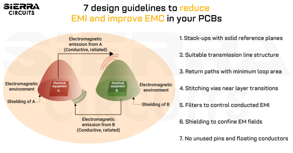
Signal integrity engineers often face challenges with characterizing signal losses and identifying the key elements controlling the performance. What do you think is the key to resolving this?
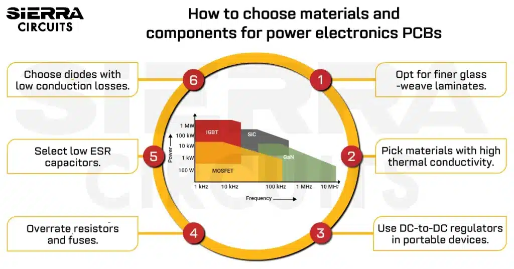
Heidi Barnes: Everyone wants to use the high-volume manufacturing processes and materials because they are easier to get, lower cost, and readily available. But I think the biggest problem is that a lot of people can get good performance by just controlling the material properties better. I used to have customers that would say, “I’m using FR4.” It could be any of a hundred different vendors. You had very little information on what the real characteristics were. Sometimes when you pay for a higher performance material, you are paying for the fact that they are controlling their manufacturing process a lot more. They are making sure that the material processes stay within a much more confined space. The dielectric constant, lost tangents, and the thickness, everything is controlled.
Thickness variation in a layer can have a tremendous impact on your transmission line impedance, which then impacts your reflection and losses. I would say, you can pay for the more expensive materials that do a much better job of controlling the properties, reducing some of the losses, and even controlling surface roughness, fiber weave, and things like that. If you want to use a less expensive material, you may have to do a little bit of legwork to figure out how I can control the material properties and confine it a little bit better. You can also get work with a manufacturer to say, “I want to use that material but how can I maybe always get the same fiber weave?”

What are the ideal materials for fabricating high-speed PCBs? Is FR-4 capable of delivering high-frequency performance?
Heidi Barnes: Anything can become a transmission line and send signals. The thing is how much loss you can withstand. Eric Bogatin says it depends on your application, repeatability, and what risk you can tolerate. Obviously, you can do a lot with FR4. I mentioned the fiber weave. That is not necessarily, with FR4, if you can get a flat fiber weave with that material then you can go a long way towards having a little bit more uniformity. Controlling the thickness of your layers is also a big deal. You can also do some tricks we used to do in the RF microwave world. It is one of the reasons why a lot of high-frequency materials like the lower dielectric constant, give you less loss but also let you widen up the traces for the same thickness. So for the same thickness of the material, you can have a wider transmission line, which then has lower losses even of the resistivity characteristics. The wider trace gives you lower losses a lot of times.
What are the simple techniques to design stack-ups for high-frequency applications?
Heidi Barnes: When designing a printed circuit board stack-up for high frequencies and for power integrity, the one that sticks in my head all the time, is obviously you have power, your electronics don’t run without power. One of the challenges is the power layers. You want to have a thicker copper, and also need to worry about the symmetry of your board so the mechanical stresses don’t cause warping. The simplest form is to put the power and ground layers in the middle. If you can get the power and the ground closer together, the loop inductance is very much smaller so the spreading inductance is less. That means I can place capacitors further from my load and still have lower inductance in the path. What hurts on the power and ground is too much dielectric between the power and ground layers.
So power and ground go in the middle and then signals to go on the outside. I am a fan of stripline running high-speed transmission lines internal to the board because then you have far fewer radiation problems. The printed circuit board manufacturing process is a lot more controllable on that edge for the transmission lines, however, you have to get in there. Via design is always a challenge and backdrilling was a really big advancement in the SI world to get rid of via stubs. Sequential lamination is another way of making sure your vias do not have capacitive stubs that can often degrade the high frequency.
How can PCB quality issues affect signal integrity and power integrity?
Heidi Barnes: I think signal integrity is an easy one. Right now at very high data rates, 56 gigabits, and NRZ, they are starting to see fiber weaving impacts. Surface roughness of the metal, and thickness variations, all these things can impact the losses. With power integrity, it is probably a little bit less of an impact, but in some of these crazy designs with 1000 amps, you start running into some fabrication issues of wanting to get thick metals for the thermal issues and the current densities. You also need the very thin layers to keep that path inductance, the parasitic inductance of the board, and the power delivery way down. I hear some manufacturers looking at sub less than one mil micron level thicknesses, and that fabrication process is not going to be easy.

Signal Integrity eBook
6 Chapters - 53 Pages - 60 Minute ReadWhat's Inside:
- Impedance discontinuities
- Crosstalk
- Reflections, ringing, overshoot and undershoot
- Via stubs
Download Now
What are the challenges involved in modeling signal integrity and power integrity?
Heidi Barnes: When modeling signal integrity and power integrity, the key is the EM simulators. The data rates for signal integrity, the lower power rails with higher currents, and the smaller margins are very sensitive to the circuit board parasitic for power integrity. Both in the SI world and the PI world, we are becoming very dependent upon the EM model to create a digital twin of that printed circuit board. The simulators are getting quite adapted to being able to bring in that PCB multilayer CAD data with the stack-up information and create the 3D model. With net-based information on the components, pins, and nets, you can quickly get up and run with ports on your EM model and look at transmission lines or power delivery networks.
Accurate simulation models can help reduce design spins for robust design solutions. Could you give us some examples?
Heidi Barnes: Accurate simulations are wonderful because they can predict behavior. They can also help you do what-ifs. In the engineering world, we used to build a hundred boards with a hundred different little variations to try to figure out which one was going to be the best. That is expensive and takes a lot of time to get results and the measurements. In the simulator, I can do a hundred experiments. I just swap the variable and outcomes to the output. Simulation can do a lot of pre- layouts, and predictive type behavior, but there are also some really interesting things going on where there are certain measurements you cannot do.
Looking for dynamic current in the power integrity world, if I want to know the dynamic current going into a multi-pin FPGA or PGA device, there are 20 to 50 different power pins, and to try to figure out what the total current is and the dynamic behavior of that is very difficult with measurement. But there are some nice techniques where I can do voltage measurements across my power delivery network and my impedance black box. Then I create that same model in my simulator and put my measured voltages across it. I can get the dynamic current, which I could not measure. It is using a digital twin, as I would call it, and combining that with some measurements to do things that you cannot do in measurement and simulation. I think that is going to be a fascinating area going forward for the simulation world.
What are the future trends in design tools and simulations?
Heidi Barnes: I should say, Keysight is doing very well right now. A couple of years ago, we came out with these PathWave EM tools called SI-Pro and PI-Pro. They are focused on the needs of a high-speed digital designer designing a PCB. What they have done, is helping to change the industry. It is making it easier for someone who is not a Ph.D. in electromagnetic theory to import a board, select the two components that they want to simulate the transmission line or the interconnect between, and have all the port setups done automatically. It knows that you are doing a printed circuit board so there is a lot of optimization and boundary conditions and setups that are done automatically, enabling a lot more people to do EM simulation and making it easier and more intuitive. It speeds up the learning process of the engineering community because now putting EM simulation at the fingertips of everybody, that learning curve just speeds up the technology they can create. The innovation you see out there in the internet of things is autonomous vehicles with all the camera systems and sensors. There is a tremendous amount of creativity as the density of electronics is bringing all of these different technologies together.
What are the key tools offered by Keysight for signal integrity and power integrity?
Heidi Barnes: Keysight works for power integrity and signal integrity. Our flagship product is Keysight PathWave ADS. We have had this, Advanced Design System simulator (ADS), for quite a few years. It was originally developed for the RF microwave world, but as we all know, signal integrity is well past. We are well into the microwave world of signal transmission. Even power integrity is not a DC problem, it is AC. You are looking at the impedance versus frequency and things like that. This ADS tool has been an excellent environment that lets you do pre-layout schematic simulations and post-layout. You have a layout tool in there. You can look at the circuit board layout design and modify things.
The benefit that has happened in the past few years is bringing the EM simulators into an environment as PI-Pro and SI-Pro integrated with ADS. It is very easy to take that layout that you have imported. You go into an EM tool, create the EM model of that printed circuit board with all the components attached, and then that EM simulator exports it back out to the ADS schematic. I can do the post-layout. What if simulations change component values? Look at what the impact is. That digital twin can also help with debugging. So once you start getting measured data, you can start feeding that back into your simulation models and increase the fidelity and start troubleshooting.
Keysight’s PathWave technology provides valuable management of the product’s life cycle from design through hardware test and production. Can you give us a brief overview of it?
Heidi Barnes: PathWave is one of the new branding names that we have given it. It is very exciting because we are looking at it. We were talking about the end-to-end design flow for a hardware engineer, starting from the concept pre-layout to post-layout of a printed circuit board, electronic design, to actual hardware fabrication and testing with instruments, and looking at what that design cycle loop looks like. I think the exciting thing with Keysight is that we are known for top-of-the-line RF microwave instruments and our scope’s amazing capability. One of the reasons also for having that PathWave phrase is that, if you look at our network analyzers, our oscilloscopes, there is an amazing amount of software, our spectrum analyzers, that provides advanced data processing and signal processing.
We are finding that we want to merge some of that capability, the data analysis that we have on our instruments, and tie that back more in with the simulation capabilities. It is becoming a little bit more blurred between simulation and measurement. I think some of the new phrases you are hearing are digital twins, where the simulation model is merging with the measurements. You are starting to get some advancement in how you design, predict the behavior and troubleshoot a PCB.
About Poulomi Ghosh : Poulomi is a microwave engineer specializing in EMI, EMC, RF, and high-speed electronics. As a senior technical writer at Sierra Circuits, she creates advanced engineering articles and webinars for hardware engineers and PCB designers.