


Contents

On-demand webinar
How Good is My Shield? An Introduction to Transfer Impedance and Shielding Effectiveness
by Karen Burnham
PCB layer count estimation allows a designer to gauge the number of signal and power layers required in a design.
Over time, circuit board layout keeps growing with constraints like rising clock frequencies, reduced area, increased number of layers, signal devices, and increase in component numbers and densities. These factors lead to an increase in board development costs.
When the design gets denser, designers find it extremely difficult to estimate the number of required layers. In this article, we explain the importance of layer estimation in design and layout. In later stages, we introduce Sierra Circuits’ Signal Layer Estimator, which makes the job easier for designers.
Why should you know beforehand the number of signal layers?
PCB layer count estimation is a vital process in board manufacturing and cost. Cost increases with the number of layers because of more production steps, more materials, and additional production time. Converting a two-layer board to a four-layer board increases the overall cost by 30-40%.
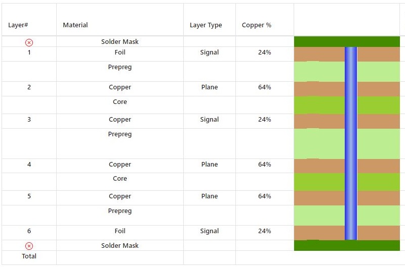
Each layer in a circuit board plays a distinct role in determining its electrical behavior. Signal layers carry electrical signals between components. The signal and power integrity will be affected by board layer configuration. Knowing the right count and how to place them creates an efficient board.
The number of layers and their sequence in the stack-up determines the construction and operation of your circuit board.
PCB Stack-Up Design Guide
12 Chapters - 55 Pages - 60 Minute ReadWhat's Inside:
- Design guidelines for HDI, flex, and hybrid stack-ups
- Stack-up representation in fab drawing
- DFM checks for layer stacks
- Characteristics of high-speed materials
- Manufacturing tolerances
- PCB stack-up examples with illustrations
Download Now
What are the different layers in a circuit board?
PCB layers are categorized as signal and power/ground planes based on the type of signal that propagates through them. The dielectric layer provides the required isolation between any two adjacent layers. Now let’s understand what these layers are.
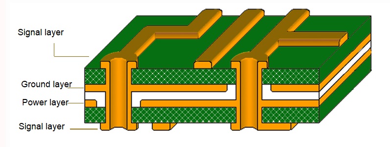
Signal layer: It is composed of etched copper traces on a layer of dielectric material. The copper traces on the signal layer constitutes the circuit (schematic) of your design.
Power/ground layer: It is a solid copper plane to which power/ground lines are connected.
Tips for arranging signal and ground planes
- Place a signal layer next to the ground plane
- Couple ground and power planes together
- Utilize buried layers located between planes to route high-speed signals
- Align traces orthogonally to reduce cross-talk between signal layers
- Adjust trace width and spacing to meet controlled impedance requirements
6 Factors that affect layer count estimation in a PCB
Knowing the layer count allows designers to select the fabrication process to achieve the desired yield. The following factors impact layer count in any board design:
1. Application
Identifying the purpose is a vital step before finalizing the number of layers in your design. The type of machines, the complexity of the electronic circuit, and the power requirements also matter a lot. Generally, the number of layers is high for high-tech applications such as Medtech and military electronics.
2. Operational frequency
The operational frequency determines the functions and capabilities of a circuit board. Multilayer boards are considered better for higher speed and operating capacity. It is crucial to find the operating frequency of the application. A multilayer board with various signal layers ensures high-speed integrity by reducing signal line inductance and parasitic capacitance. In the inner layers, when signals are routed as stripline traces, they have ground planes on the top and below. This gives better signal integrity and reduces cross-talk.

3. Thermal dissipation
More copper layers offer more thermal paths for heat to flow away from the sources, so a large board surface is used for heat dissipation to the environment. A double-layer board with the same circuit gets hotter as compared to a multilayer board.
4. Pin density
The number of layers depends upon density and signal layers. The pin density defines the number of pins per square inch. As the pin density increases, the number of layers increases.
5. Board thickness
The board thickness increases as the layer count increases to accommodate the minimum thickness of materials used. The aspect ratio (board thickness to the smallest hole diameter) also matters.
6. Design complexity
The total number of layers required for a given design is dependent upon the complexity of the design. Design complexity and power levels decide the number of layers. As mentioned earlier, adding more layers increases production costs but enables the inclusion of more tracks. Complex boards with advanced functionality manufacturing costs increase with more layers.
Layer count estimation is one of the crucial steps to achieving design success. As seen in this section, there are numerous attributes that impact the number of layers in your circuit board.
This calculation can sometimes be complex and time-consuming. To overcome this challenge, Sierra Circuits has developed Signal Layer Estimator.

How to use Sierra Circuits’ Signal and Plane Layer Estimator
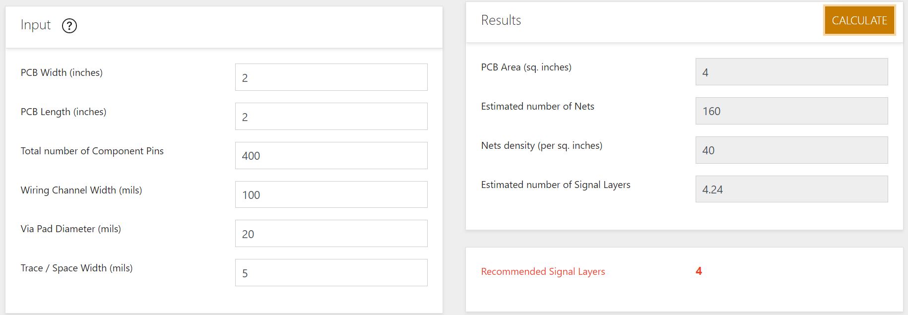
The Signal Layer Estimator has two sections: input and results. You will have to fill in the values of all the input parameters to view the recommended number of signal and power layers.
Input parameters for the estimator
- PCB width (in inches)
- PCB length (in inches)
- Total number of component pins
- Wiring channel width (in mils)
- Via pad diameter (in mils)
- Trace/space width (in mils)
Once you provide the necessary data, hit calculate in the results tab to view the prescribed number of signal layers along with the following attributes.
- PCB area (in sq. inches)
- Estimated number of nets
- Net density (per sq. inches)
Sierra Circuits’ Signal Layer Estimator makes use of several algorithms to calculate the minimum number of signal layers that are required to accomplish every interconnection in a board layout.
Algorithms to compute signal and power layers
The following algorithms help to estimate the number of signal and power layers in a board:
- COOR’s wiring length model
- Hannemann’s wiring demand model
- Geometric model (Moreseo)
A clear understanding of the signal layers count helps to determine the overall time and the manufacturing cost. The Signal Layer Estimator calculates the optimum number of signal and power layers. Do let us know in the comment section if you have any questions regarding PCB layer count estimation.
Refer to our DFM guide to learn the design for manufacturing aspects.


