Contents

On-demand webinar
How Good is My Shield? An Introduction to Transfer Impedance and Shielding Effectiveness
by Karen Burnham
Miniaturization of the copper features in electronic circuits results from placing interconnections closely with a high packing density. As a result, crosstalk in the HDI PCB substrate comes into play because of the increased coupling between the adjacent signal lines.
HDI substrates are multi-layer, high-density circuits with features including fine lines and well-defined space patterns. The increasing adoption of HDI substrates enhances the overall functionality of PCBs and limits the operational area.
One of the key factors that differentiate HDI PCB design from the rest is its unique design that comprises multiple layers of copper-filled microvias. These multi-layers of microvias enable vertical interconnections. Further, HDI substrates offer the advantages of having higher integration levels and better placement of components on both sides. Additionally, HDI boards consist of a higher number of I/Os in smaller geometries. Other features of HDI substrates include faster transmission of signals and a significant reduction in signal loss and delays.
The recent technology adopted for fabricating HDI boards deals with the miniaturization of components and the adoption of high-end devices. However, signal integrity challenges in HDI, such as crosstalk, can severely affect the performance of HDI boards. Thus, adopting advanced PCB design services becomes critical to avoid crosstalk in HDI boards.
What is crosstalk in PCBs?
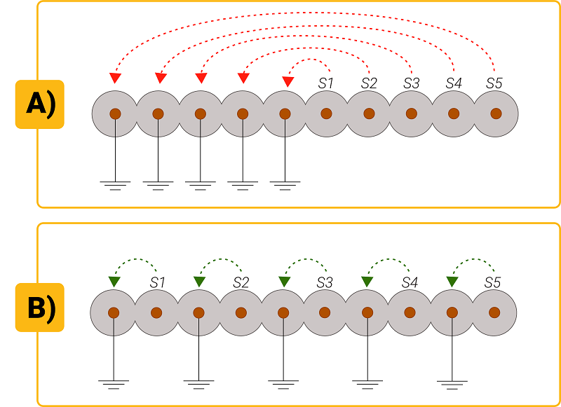
Crosstalk is an unintentional electromagnetic coupling among the traces on a PCB (even though they are not in physical contact with each other). Moreover, electromagnetic field disturbance can take place in PCBs due to external interference.
Crosstalk occurs when there is coupling (capacitive and inductive) of energy from the aggressor signal to the victim signal (typically, two tracks close to each other) regarding the interference of electric and magnetic fields. The electric field is coupled via mutual capacitance between the signals. On the other hand, the magnetic field is coupled via mutual inductance between the signals. Traces running parallel on the same layer or running parallel vertically between two layers are susceptible to crosstalk.
What is the crosstalk effect?
Crosstalk generates undesirable effects that affect the clock, periodic signals, and system-critical nets like data lines, control signals, and I/Os. Additionally, the affected clock and periodic signals create serious functionality concerns for working PCB and assembly components.
Due to the crosstalk effect, the voltage and current levels reach the threshold level of the logic devices. This can be interpreted as a false logic state when it reaches the receiver. A designer needs to work smartly to avoid the errors caused by these erroneous logic states. Crosstalk can also affect analog signals by adding noise. This noise could come through the power rails.
Also read: Happy Holden Discusses HDI
How is crosstalk minimized in HDI substrates?
Crosstalk in HDI substrates is reduced by the shorter coupled lengths and by the lower dielectric constant by as much as 50 percent. Other factors that can limit crosstalk in HDI substrate include,
- Use of lower Dk materials.
- The lower dielectric constant of the HDI PCB material system may allow a board to shrink up to 28 percent.
- The thinner the distance to the reference plane, the lower the near-end crosstalk will be.
HDI miniaturization provides shorter interconnect lengths. Crosstalk in HDI substrates can be reduced if a lower dielectric constant material is used.
Eric Bogatin, Signal Integrity Evangelist at Teledyne LeCroy, explained, “A typical line-width in HDI technology is 3 mil (75 microns). The figure below shows the characteristic impedance of 3-mil-wide traces for various dielectric thicknesses.
The dielectric thickness will be less for a lower dielectric constant. This means a lower dielectric constant material system will either result in less crosstalk for the same spacing, or the traces can be moved closer together and have the same amount of crosstalk.”

The type of materials you use defines the quality of your end product. Download our PCB Material Selection Design Guide to learn how to choose the right material for your designs.

PCB Material Design Guide
9 Chapters - 30 Pages - 40 Minute ReadWhat's Inside:
- Basic properties of the dielectric material to be considered
- Signal loss in PCB substrates
- Copper foil selection
- Key considerations for choosing PCB materials
Download Now
Case studies by Eric Bogatin
Eric Bogatin continues, ”In the two cases studied, the line width was 3 mil, and the dielectric thickness was adjusted so that the line impedance was the same for the two different dielectric constants. From these curves, it can be seen that if the routing pitch is crosstalk-constrained, the lower dielectric constant of the HDI material system may allow a board to shrink up to 28 percent.
The magnitude of the near-end voltage noise will scale with length for coupled lengths less than the saturation length. The saturation length will depend on the rise time. For a rise time of 1 nanosecond, the saturation length with an effective dielectric constant of 2.5 is about 7.6 inches, which would include many of the traces in a small card application. The relative coupled near-end noise would be given by:

Crosstalk in HDI substrates is reduced by the shorter coupled lengths and by the lower dielectric constant by as much as 50 percent. Shorter trace lengths will radiate less, and traces with thinner dielectric will also radiate less. The example below shows that the shorter coupled length leads to less mutual inductance (Lm), and thinner traces lead to less mutual capacitance (Cm).

The thinner the distance to the reference plane, the lower the near-end crosstalk will be, or the same crosstalk for a longer coupled length. With length reductions of 2x and dielectric thickness reductions of 2x over conventional boards, the radiated field from HDI signal loops might be reduced by as much as 4x, 12dB.”
Eric Bogatin states, “If the entire board is HDI, rather than just a few outer layers, controlling the return path can be a bigger challenge than in through-hole boards.” See the case study on designing an HDI board with 0.4 and 0.65mm BGAs to learn how we properly ground a 0.4mm BGA with high pins.
Key takeaways by Eric Bogatin
“You have to pay attention to the same issues to deal with crosstalk in HDI substrates:
- Providing a continuous return path
- Engineering controlled impedance interconnects
- Route in a linear, daisy chain path with minimal stub lengths
- Control reflection noise with terminations
- Manage via to via crosstalk by the return path control
- Use low-inductance capacitors connected to the IC pins
In conjunction with a through-hole core, HDI interconnects can be incredibly valuable.”
Also read: The History of High Density Interconnect
Design techniques to avoid crosstalk in HDI substrate
The following measures can be adopted to avoid crosstalk in an HDI substrate:
Minimize the capacitive coupling
In integrated circuits, capacitive and inductive coupling cause crosstalk. Inductive coupling is concerned with mixed input-output circuitry, while capacitive coupling affects the switching speed of the circuitry. Here are some considerations for circuit design to reduce the capacitive coupling, thus crosstalk:
- Do not route two parallel wires over a long distance in the same layer. Also, the layers adjacent to the traces should be perpendicular.
- Route ground or power between two sensitive signal lines.

- Separate sensitive nodes from full-swing signals and avoid floating nodes. Nodes sensitive to cross-talk issues should be provided with devices to minimize impedance.
- Use differential signaling on sensitive low-swing wiring networks.
- Crosstalk between the signal layers in different layers can be reduced by designing a ground layer between the signal layers.
- On inner layers, when signals are placed between two ground layers, the capacitive coupling is reduced. Read how can we reduce parasitic capacitance in PCB layout.

- PCB designers can use optical interconnections to reduce EMI and crosstalk. Read more about PCB design guidelines for EMI and EMC.
Download the HDI PCB Design Guide for guidelines on designing high-density circuit boards. This e-book will help you plan your stack-up with microvia structure, choose the right materials, and manage signal integrity and controlled impedance requirements.

HDI PCB Design Guide
5 Chapters - 52 Pages - 60 Minute ReadWhat's Inside:
- Planning your stack-up and microvia structure
- Choosing the right materials
- Signal integrity and controlled impedance in HDI
- Manufacturing considerations for higher yields
Download Now
Reduce the inductive coupling by reducing the ground-power loop area
The ground plane is the low-impedance return path for the signal conductors. Designers must reduce the area between the ground and the signal conductor to minimize the loop. A reduced loop area can reduce the inductance.
In the ground plane of a multi-layer PCB, there must be a large number of vias, which increases the via density. Inductive coupling could occur in a group of adjacent connections if the ground and signal layers share a common area. Designers must route a wide loop around the slot to avoid inductive coupling and thus reduce crosstalk.

A via surrounded by a closed ground wall shortening the planes acts as an electrical boundary. It reflects all the energy and develops half-wave resonances based on the diagonal dimension of the closed boundary.
Provide the return path as close as possible to the signal path
Special care must be given to ground pins and wires when using connectors and cables since we don’t want to increase the current return loop area. Moving the ground pin close to the signal pin can minimize the loop area.

Avoid nested loops using ground pins
While designing cable inputs, running different conductors nearby may generate coupling issues. Using the same pin for the ground path from several signals creates nested loops with high mutual inductance. The PCB designers must consider separate ground return pins, which should be at a minimum distance from the signal pins to reduce the inductive coupling.

Opt for every layer interconnect (ELIC) construction
Every layer interconnect (ELIC) is an advanced stack-up construction method in which a connection can be started or ended in any layer. Circuit connections are made in the initial buildup itself, so there will be only fewer requirements for blind and buried vias. This gives the designers a large routing space in the layers. However, there are some limitations when it comes to the routing of an ELIC construction.
The designers should care about the signal layer; no two signal layers should be adjacent. Place the ground layer between all signal layers. As the ELIC construction allows connection between layers, it is easy to build up in a symmetrical arrangement.
Use boulevard structure via placing for crosstalk reduction in HDI substrate
A boulevard structure via placing is used to reduce crosstalks and increase routing density. According to their application for via-to-via crosstalk, designers can use several types of via-placement structures in BGA. A boulevard structure suitable for reducing crosstalk and increasing routing space is shown above. Let us discuss that.

Region 1 consists of the outer rows, where the number of rows varies from 4 to 6 per the design rules. Region 2 consists of all the inner rows. Region 3 is the transition between inner and center rows, and region 4 is the center.

As depicted above in region 1 a, the traces are routed on layer 2 to the maximum routing density using a 1:2 microvia. To increase the number of vias or to reduce the spacing between them, designers can bring the vias closer to the ball pad without exceeding the minimum distance required. Also, designers can change the orientation of the via-ball pad structure. Such arrangements are capable of increasing routing space and reducing crosstalk between vias.
After routing outer layer BGA pins using 1:2 microvias in region 1, rows from 4 to 6 in region 2 b are routed on layer 3 with maximum routing density using 1:3 skip-vias. The skip-via allows a connection from Layer 1 to Layer 3 without using a pad on Layer 2. This pattern can also be changed by moving the via closer to the ball pad and adjusting the angle to reach the required size.
Region 3 c is the transition region between region 2 and region 4. It can use any of the 1:2 and 1:3 microvias as per the routing strategy. Region 4 d is the leftover region. Usually, the central region is occupied by ground and power pins. To allow the greater ground plane fill on layer 1, vias cannot be placed in the exact center of the BGA.
Like this, dividing the BGAs into regions to place vias not only increases the routing density but also reduces the number of layers. If the nets end in blind vias instead of via stubs, via crosstalk can be reduced. To know more about via stubs read how via stubs affect signal attenuation and data transfer rates.
Note: In the above BGA pattern example, we have used an orthogonal short dog-bone structure. You can also use other angle adjustments based on the via sizes.
See how to breakout a .5mm BGA for more.
Use dual offset coplanar stripline structure for HDI crosstalk reduction

We all know that conventional PCB designs use a dedicated power plane. But as soon as the density and the number of voltage rails increase, the need for split planes arises. We can use two orthogonal layers to distribute PWR as a ‘mesh structure.’ By placing signals between the different voltages, we can increase the number of split planes for up to eight different voltage rails. It is called a ‘dual offset coplanar stripline with a separate GND reference. This structure provides lower crosstalk and voltage to all the components from LAYER 2 to LAYER N-1 using only a blind via.

Scaling PCB geometry for crosstalk reduction in HDI substrate
Crosstalk can be described based on two figures of merit, named the Near-End Crosstalk (NEXT) coefficient and the Far-End Crosstalk (FEXT) coefficient. Both terms give the ratio of near and far-end noises generated on the noiseless line in a uniform pair of transmission lines when the ends are terminated in their characteristic impedances. It is a measure of the typical crosstalk noise that would be observed.

The characteristic impedance can be defined by dielectric thicknesses, line width, and dielectric constant, while the space between the adjacent traces tells the crosstalk. These electrical qualities scale with geometry. For example, if every feature in the cross-section is reduced by a factor of 5, the characteristic impedance and NEXT and FEXT values will not change. Check the following geometric features for a conventional PCB and an HDI interconnect. They reflect the same performance.
| Geometric features | Conventional PCB | HDI |
|---|---|---|
| Dielectric thickness | 5.1mils | 1.02mils |
| Line width | 10mils | 2mils |
| Copper thickness | 0.5oz | 0.1oz |
| Dielectric constant | 4 | 4 |
Sometimes, designers think that scaling doesn’t give any electrical advantage to HDI designs. Because scaling all the features down still reflects the same electrical performance. It is valid for scaling down a cross-section of uniform signal lines. Still, there are two non-scaling terms that affect electrical performance in HDIs:
- The short length of the HDI interconnects
- Use of non-reinforced laminates with a lower Dk in HDI interconnects
The above features provide shorter and controlled time delays and less crosstalk since some electrical properties do not scale with smaller feature sizes.

Impact of stack-up geometry and coupling length on HDI crosstalk
The magnitude of far-end crosstalk also depends upon the stack-up geometry and the coupling length. It varies like:
FEXT = k (Len/RT)
Where FEXT = Far-end crosstalk coefficient
k = Coupling between two lines (victim and aggressor) in ns/inch
Len = Coupling length (inches)
RT = Rise time of the signal (ns)
Far-end noise is generated due to the inconsistency in the dielectric layer at the surface interface. This non-uniform nature of the dielectric constant increases the far-end noise. However, only surface traces experience the far-end noise, and buried traces (like in the stripline) experience only near-end noise. It is worth noticing that near-end noise saturates in magnitude and does not scale as coupling length increases. It only happens if the coupling length is more than the critical length.
Eliminating crosstalk in HDI substrates before EMC testing provides PCB designers with a faster time-to-market period for their products. Crosstalk is one of the critical parameters that create signal integrity issues if not treated well. It can directly lead to distortion in the receiver signal. The crosstalk amount depends upon the line spacing, signal rise time, amplitude of the aggressor signal, and board and trace geometry. Thus, minimizing the effect of crosstalk in HDI substrates should be a prime concern among designers.
We manufacture and assemble HDI PCBs with blind, buried, and micro-vias, built-up laminations, and the highest signal integrity in the industry.
Need assistance in designing your HDI PCBs? Post your queries on our forum, SierraConnect, and our experts will resolve them.