


Contents
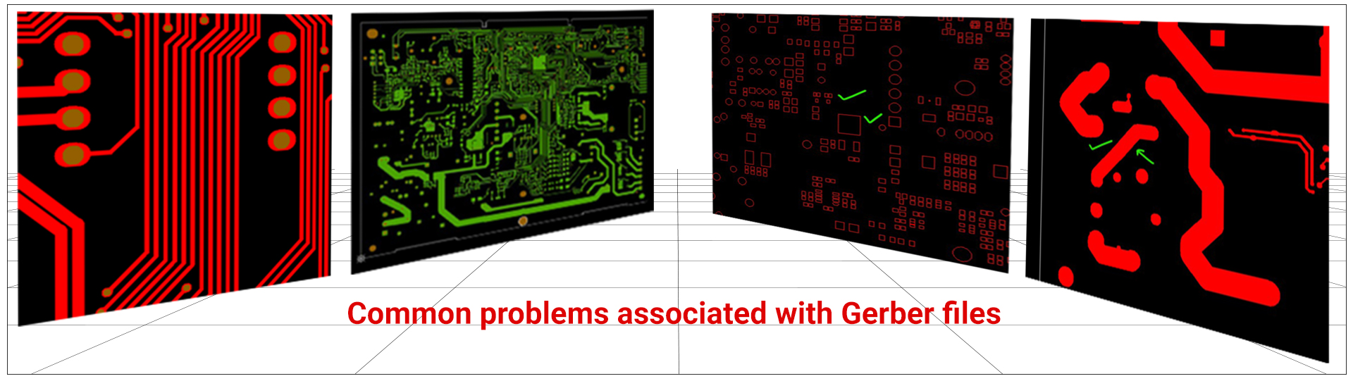
The most common problems seen in Gerber files include design mismatch, insufficient clearances, obsolete file formats, unregistered layers, and incomplete files.
Gerber files are the output of the circuit board design process. These files are utilized for the PCB manufacturing and assembly process. Gerbers provide information about each and every layer in the board stack-up.
Design for manufacturing (DFM) involves checking the Gerbers for errors, assuring their manufacturability, and meeting the requirements of the manufacturer. Hence, it is essential to ensure that these files are created with the highest amount of precision. Let us have a look at the errors most commonly seen in these files.
What is a Gerber file and what is its purpose?
Gerber files are digital blueprints of a PCB that contain layer-by-layer details that are utilized by circuit board manufacturers. These files come in open ASCII vector format and describe the physical attributes of each board layer.
They include layer images to create films for manufacturing stages, such as inner layer imaging, etching, etc. These files are converted to CNC-compatible files using a laser process, which also hardens the photoresist.
Gerbers are used to analyze all layers in a PCB. These files are required for board assembly and inspection as well. Apart from this, stack-up planning is also carried out based on these files.
Once the Gerber is analyzed, CAM will produce output files for various manufacturing departments. There are several output files, including drill program (sub drill and main drill), imaging layers, solder mask output, route file, and IPC netlist.
How to verify Gerber files
There are multiple ways to verify these files. The significant ones are described below.
Manual method
- Load the files using a Gerber viewer.
- Take printouts of the files on a scale of 1:1.
- Using this scaled version of the circuit board, place the parts directly on the printout. This will help verify whether the footprints were created in the right manner or not.
- Give special care to check the quad flat packages (QFP) since any mistake, in this case, is disastrous.
- Visually check if the spacing between the traces and pads is sufficient.
Automated method
In this method, Gerber files are loaded into a DFM software tool. This software checks parameters such as trace-to-trace gap, trace width, the distance of the trace from the edge of the board, silkscreen overlapping pads, and so on.

What are the common Gerber file issues and how to fix them?
The common issues that are seen in Gerbers include design mismatch, insufficient clearances, obsolete file formats, etc. Let us take a look at these in detail.
PCB design doesn’t match the manufacturer’s capabilities
It is important to create an efficient board design that is innovative, efficient, and manufacturable. At the same time, this design should match the fabrication capabilities and techniques of the intended manufacturer. Otherwise, the contract manufacturer will end up reaching back to the designer requesting an altered design. This will lead to a waste of time and effort.

Design for Manufacturing Handbook
11 Chapters - 96 Pages - 90 Minute ReadWhat's Inside:
- Annular rings: avoid drill breakouts
- Vias: optimize your design
- Trace width and space: follow the best practices
- Solder mask and silkscreen: get the must-knows
Download Now
Insufficient clearances between trace and pads
Sufficient clearances between traces or between traces and the pads must be provided in the design. Moreover, there should be adequate clearance between the drill hole and the copper area (drill to copper). If not provided, this will lead to shorts in the inner copper layers of the board. The same condition may also occur when the minimum clearance between a drill hole and the adjacent inner copper layer is less than the required value (8 mils).
Obsolete file formats
Gerber files that have a 274D format are better left alone. These files won’t work with the current fabricators. An RS-274X Gerber format or an updated version known as Gerber X2 format is used in the current market. ODB++ design files are also used for fabrication. It is generally a good idea to check with the board manufacturer beforehand about the file format that they accept.
Incorrect drill file format
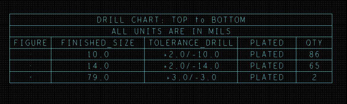
Without the right format of the drill files, it is difficult for circuit board fabricators to import the Gerber file. These files are used to identify the size and location of the hole that has to be drilled. Drill files contain information that can be translated directly to the CNC machine.
Many CAD software packages have the option of generating drill files. The header of these files should indicate the format. Such a format is known as a numerically controlled (NC) drill file. They usually have ‘.xln’ or ‘.drl’ or ‘.ile’ extension.
Drill file extensions
| Extension | Description |
|---|---|
| .DRL | Details of blind and buried vias |
| .DRR | Details about hole size, count, and tool travel |
| .TXT | Drill files in ASCII text, contains details of PCB design and separate file hole types |
| .LDP | Drill pair report, used by the CAM Editor to detect blind and buried vias. |
Absence of fabrication drawing
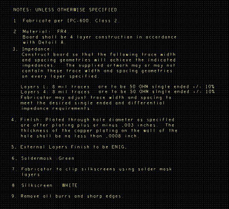
It is highly recommended to provide a fabrication drawing to the manufacturer. It provides essential information about board details that may not be present in the Gerber files. It contains information such as the overall dimensions of the board, special cutouts, and routing.
In addition to this, Gerber files also contain information about the fabrication of the board, such as file name, the thickness of the material, the type of material, the finish of the material, and so on. This information is termed as fabrication notes. An example is shown below.
Unregistered layers
All Gerber files need to be registered to a common data point. These layers have a specific alignment. This requires extra time and is prone to errors. There should not be any unregistered layers at the time of submission.
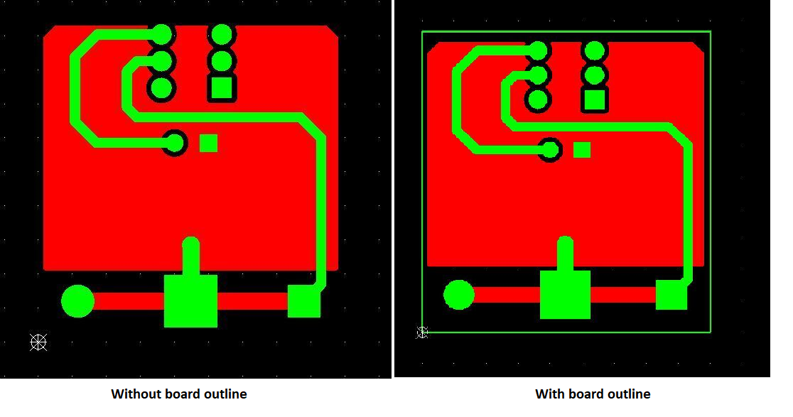
Missing board outline
Gerber files should have a clearly defined board outline. A board outline defines the dimensions of the PCB based on the customer’s requirement. It gives information about the exact bounds of the board edge which is required by the fabrication machine to route the individual boards from the panel.
If the board outline has not been provided, there is are high chance that the manufacturing is put on hold by manufacturers.
Some CAD software packages don’t produce outlines by default and must be instructed to produce one. It can be a part of the Gerber file or a general drill file.
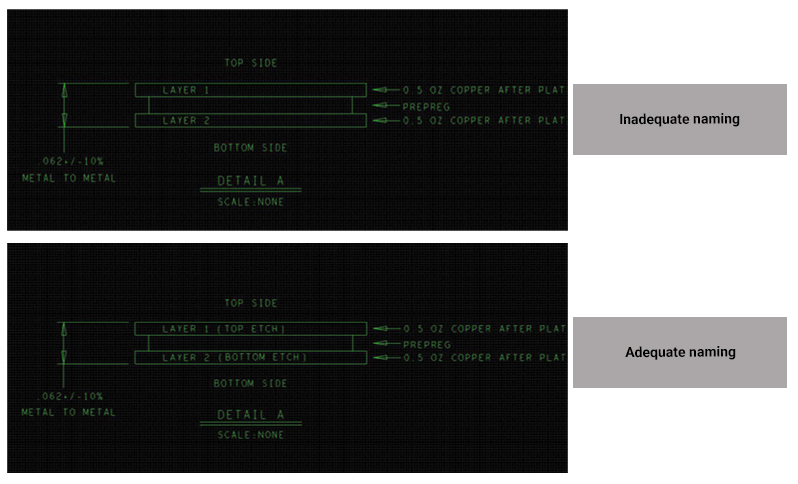
Unorganized file labels/names
Gerber file labels should always be in the right order to interpret easily. Use an established naming protocol that can be understood by the manufacturer. This way, it will be easier to identify the files required without ambiguity.
This can be done by providing a simple PCB stack-up and describing the order of copper layers. This stack-up can also be included in the fabrication drawing, or as a PDF file or an Excel file, or as a layer in the Gerber file.
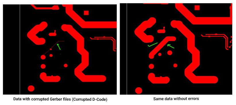
Corrupted Gerber file
A cursory look gives away some of the errors in the Gerber data. To get a detailed analysis, use a Gerber file viewer that ensures proper matching between generated files and the original design. The data errors can be avoided if the settings in the CAD software are carefully set, and file generation is rightly mentioned.
Empty Gerber file
A designer may end up creating Gerber files that have no information in them. These are known as zero-byte files. A manufacturer reading these files wouldn’t be able to identify if the file is added by mistake or if the information in the file was deleted accidentally. Hence, it is important to check every Gerber file contains all the relevant information.
Design files mismatch
The PCB design process works in multiple stages, and until the required result is achieved, multiple improvisations are made. These may result in disparities in the design files, as well as a delay in production.
Hence, before the board designs are submitted, revisit the improvisations, fabrication drawings, assembly drawings, and other design components. This ensures the matching of all the design files.
Wrong CAD settings of Gerber viewer
Certain CAD software may split a single copper layer into multiple Gerber files. This is prevalent in layers that contain filled areas since the software generates one file for the copper pour, one for the traces, and one for clearances.
Therefore, it is important to make sure that before submission, the files with a Gerber viewer have the right CAD software settings. Wrong settings lead to the unintended splitting of a single-layer file.
Composite layer does not map to a single layer
At times, composite layer images are created during the generation of an individual layer based on the design specifications. In these cases, it is vital to combine the images in such a way that one Gerber file is mapped to one single layer to avoid errors.
Vectorized pad
Vectorized pad occurs on the surface mount pad of the solder mask or the paste mask layer. CAD may generate a cluster of small vectors that are bound together to form a pad rather than generating a pad as one solid object (that would be associated with the Gerber file).
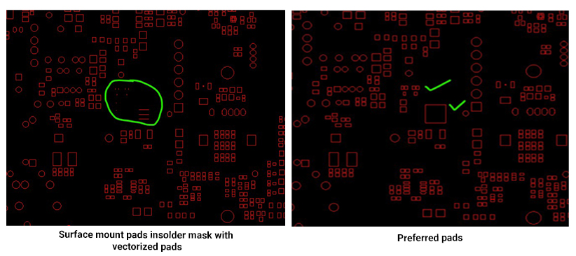
This issue can be addressed, but it is time-consuming. An efficient way is to set the software to generate ‘flash pads’ instead of ‘vector pads.’
Incomplete file
A manufacturer needs to know every specification associated with a circuit board, ranging from the size of plated-through holes, layer information, dimensions of the board, and so on. In case some information is missed out, it would result in a mismatch with the desired specifications.
Hence, ensure that the Gerber files are in the right place and are easily accessible.
Multiple aperture lists
A Gerber file should have a single aperture list that contains details required by the manufacturer. This consists of tools required during every stage of fabrication. If multiple aperture lists are present, it can be chaotic and error-prone and will slow down the process of manufacturing.
Gerber file errors can be avoided easily, and special care should be taken to ensure the above-mentioned problems are addressed. With the help of sophisticated tools like CAD and DFM products, it is possible to reduce the potential errors in the design.
Also read how to export gerber production files in altium designer to learn the step-by-step process to generate accurate Gerber files for seamless PCB manufacturing.
Let us know in the comments section some of the Gerbers issues that you face, and we will try to solve them for you.


