


Contents
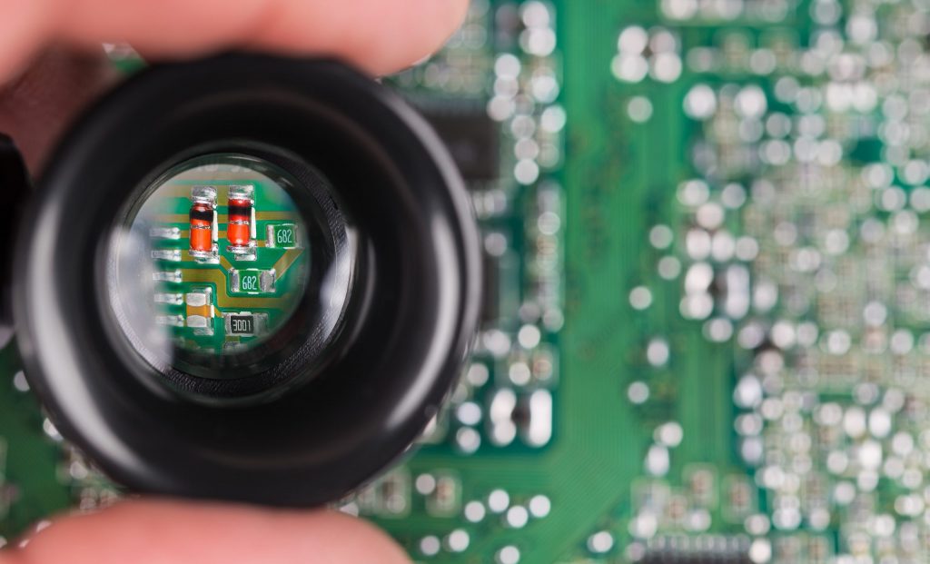
The main agenda of using HDI technology is to pack more components on a smaller board. Choosing smaller footprints for HDI increases board functionality and component density.
Therefore, while designing a high-density interconnect board there are many problems to tackle. Usage of components with smaller footprints enables a dense accommodation.

Signal Integrity eBook
6 Chapters - 53 Pages - 60 Minute ReadWhat's Inside:
- Impedance discontinuities
- Crosstalk
- Reflections, ringing, overshoot and undershoot
- Via stubs
Download Now
What is an HDI layout?
An HDI layout accommodates more components within limited board space. This design faces the below-mentioned challenges:
- The board workspace area is limited
- Usage of smaller footprint components
- Denser spacing between components and other physical features
- Increased number of components on either side of the circuit board
- Longer traces increase the signal propagation delay
- Boards will require more trace routes
The choice of via types significantly impacts the high-density layout. There are no hard and fast rules regarding the type of via used in HDI boards. The designer has the option to choose from blind/buried microvias to the conventional through-hole ones.
The blind/buried microvias can be arranged as staggered or stacked, as per the board design requirements. The choice of vias will determine the process duration, steps, and cost. Hence, these factors should be considered to optimize the cost and manufacturing complexity.

HDI PCB Design Guide
5 Chapters - 52 Pages - 60 Minute ReadWhat's Inside:
- Planning your stack-up and microvia structure
- Choosing the right materials
- Signal integrity and controlled impedance in HDI
- Manufacturing considerations for higher yields
Download Now
Component selection for high-density interconnect
The component selection is a time-consuming process during HDI design. The components that are mounted on the circuit board will decide the trace width, routing requirements, drill hole sizes, and stack-up. The limited area available on the PCB restricts the size of the component footprint. At the same time, fine-pitch components will increase the number of layers required for proper routing. Thus, the optimization between these two factors will provide an ideal component size.
Performance, package or land pattern, traceability, and availability are the four factors that determine the selection of an HDI component.
Importance of proper component placement
The placement of components affects the board’s operation and efficiency. When it comes to HDI, the components will be closer than the conventional layout. Even when the components are closer to each other, no EMI should occur. This will reduce the signal efficiency of the traces. Also, parasitic capacitance or inductance should not occur between the adjacent pins or pads. Therefore, the possibility of signal integrity improvement has to be properly studied before placing the components on the PCB.
The via locations are also dependent on the component placement. Therefore, if the via locations are asymmetrical, it might lead to uneven stress across the board. As a result, the board’s strength will be affected.
Check out our tutorial on how to place components in KiCad.
What are HDI PCB footprints?
Component footprints are the patterns on the board layout that represents the location of components that will be soldered during circuit board assembly. There is no particular category of footprints specifically designed for high-density interconnect boards. Designers try to make the component footprints smaller so that less space is consumed. As per IPC-7351, the footprints, in general, are classified into three categories.
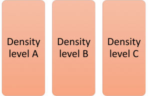
- Density level A: This classification of footprints is meant for low-density product applications. Wave soldering is best suited for density level A components. These footprints occupy more board area compared to the other two.
- Density level B: This section applies to component footprints for boards with a moderate level of component density. The density level B footprints offer a robust solder attachment condition in case of reflow soldering. These footprints are of nominal size.
- Density level C: These footprints are meant for high-density boards like HDI. The size of these footprints will be smaller compared to levels A and B.
Now, we have realized that density level C footprints are the smallest in land occupancy and are best suited for high-density interconnect boards. But before we decide which one to use, these footprints should satisfy the IPC-7351 criteria. They should also comply with the fabrication and assembly capabilities of the vendor. See our case study, eliminating BOM and footprint errors in PCB assembly to understand the common mistakes to avoid while designing a footprint.
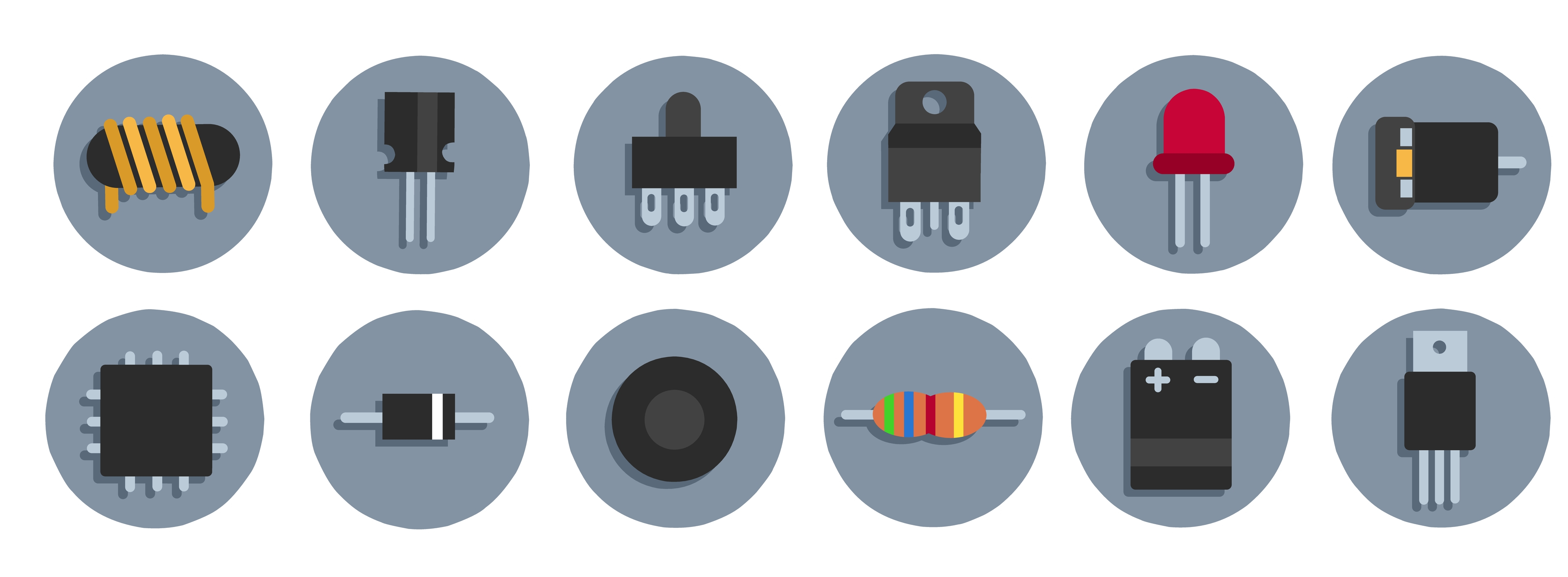
SMD packages with smaller footprints for HDI
SMD packages with smaller footprints are best suited for HDI boards. Some of the examples are 0402, 0201, 001005, etc. The dimensions of these packages are provided below.
| Package type | Dimensions in mm | Dimensions in inches |
|---|---|---|
| 0402 | 1.0 x 0.5 | 0.04 x 0.02 |
| 0201 | 0.6 x 0.3 | 0.02 x 0.01 |
| 01005 | 0.4 x 0.2 | 0.016 x 0.008 |
Resistors and capacitors are generally available in these miniature SMT packages. Surface-mount inductors are available in 0805 (2.0 x 1.3 mm) and 0603 (1.5 x 0.8 mm) packages. There are other components like transformers, quartz crystal resonators, ceramic resonators, filters, and so on that are not available in these extremely small package styles. But we have to ensure that these components are compact and compatible with the pick and place machinery, irrespective of the component package style.
To learn how smaller footprints can mitigate HDI routing issues, see 5 HDI PCB routing challenges with solutions.
Less-space consuming standard IC packages
When it comes to IC packages, the smaller versions are listed below:
Small outline packages (SOPs)
-
- TSOP: Thin small outline package that comes with 0.5mm pin spacing.
- SSOP: Shrink small outline package with a pin spacing of 0.635mm.
- QSOP: Quarter small outline package with 0.635mm pin spacing.
- VSOP: Very small outline package with 0.4, 0.5, or 0.65mm pin spacings.
BGA
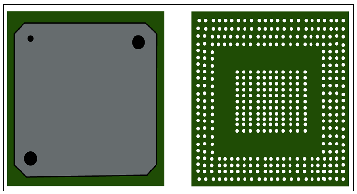
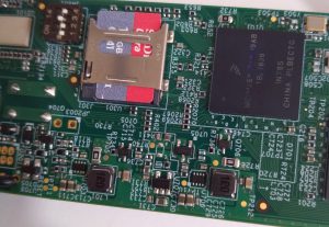
BGA packages are commonly used in HDI boards. The fine pitches of these components and implementation of via-in-pad technology help serve the compactness required in these types of circuit boards. Since the pins are under the component’s surface, the space consumption by these components is even reduced. BGA components with pitches as small as 0.4mm, 0.5mm, and so on are available.
See our articles to understand how to breakout a 0.4mm BGA and how to breakout 0.5mm BGA here.
QFP
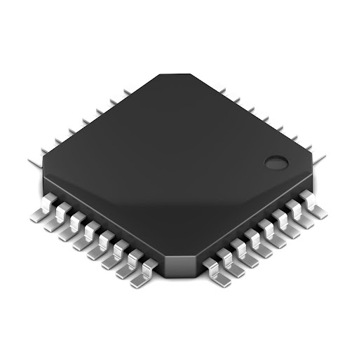
Quad flat packages also offer some variants that are ideal for use in high-density applications.
-
- LQFP: Low-profile quad flat packages come in a low profile and are available in varied pin spacings. The height remains at 1.4mm.
- TQFP: Thin quad flat packages are thinner versions of the usual QFPs with smaller form factors.
QFN
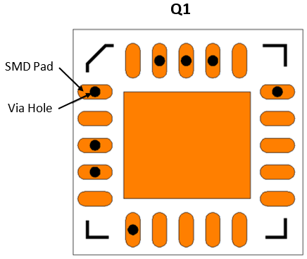
Quad flat no-leads packages are suitable for HDI because of their small footprints, input-output pads at the perimeter, and thermal pads. Therefore when the routing is congested and placement is dense, these packages will dissipate heat easily. Micro lead frame QFN package is an example of a miniature variant that has an average height between 0.35mm to 1.45mm.
Thus, from all of the topics discussed above, we can summarize the following aspects about the component footprints in HDI:
- The component density per square inch of an HDI board is always greater than a convention board.
- Use high-pin count and low pitch components.
- A smaller footprint brings components closer to each other which results in cutting down the signal path length and hence improves the signal quality.
- The component footprint should always follow the IPC-7351 standards and also the DFM requirements of the fabricator.
- Use via-in-pads for routing the components.
If you have any queries regarding HDI component footprints, please let us know in the comment section below.


