NOTICE: We've reduced the cost of our PCB design services by 20%.
Request a quote today, and you'll automatically receive our new, lower pricing.
Sierra Circuits Helps You With Your PCB Design
You have a brilliant idea for a PCB, but you’re short on time and low on resources? And you’re looking for PCB design support to handle the complexity and the challenges of your project, and deliver a board that meets your expectations and your deadlines?
That’s where Sierra Circuits comes in.
We offer PCB design support to help you create high-performance, market-ready boards for any industry, application, or specification. Backed by a team of seasoned engineers with over 30 years of experience, we can help you finish your designs on time.
Our support turnaround time varies on the complexity of your designs, for simple 2-4 layers we take 4-5 days, and for more complex designs our team takes up to 8-10 days. Rest assured, you don’t have to wait a lot as our designers are ready to start providing support on your projects immediately, ensuring timely and efficient delivery of your PCB designs.
What Makes Sierra Circuits Different?
We are not just another PCB company. We are your all-in-house partner. We care about your success and satisfaction, and we work with you every step of the way to make sure your design meets your requirements and exceeds your expectations.
But that’s not all. We also offer a complete range of PCB services that cover every aspect of your project, from design support to assembly. Once you’re satisfied with your designs, you can raise a quote with us and get your circuit boards delivered just in time.
Thanks to our single facility for fabrication and assembly which eliminates the need for multiple PCB partners, and this does not end here. Sierra also helps you with sourcing and stocking the right components for your future needs in our warehouse. We go one step further and offer advanced testing to ensure that your boards meet the quality standards and offer high performance.

We Support You At Every Step Of Your PCB Design Journey
One of the core benefits of working with us is, you can request design support at any particular stage, you can consult our experts and get a customized design support quote.
We take care of all the challenges of your PCB projects, whether they’re related to design support or fabrication and assembly. So that you can save your time and focus on other important things.
What’s New at Sierra?
-
Discover Our New Design Support That Will Solve All Your PCB Design Problems.
-
At Sierra, we never stop innovating and improving our PCB design support to meet the evolving needs and expectations of our customers. That’s why we are excited to announce our new design support that will take your PCB projects to the next level.
Choose From a Wide Range Of Our A to Z Design Support Solutions
Concept to Prototype Design Support
Let’s bring your innovative ideas to life with Sierra’s comprehensive concept to prototype service that guides you through every stage of this transformative journey.
Our concept to prototype service includes:
-
Schematic Design Support
-
BOM Validation
-
Footprint Design Support
-
Stack-Up Design Support
-
Layout Design Support
-
Firmware Design Support
Footprint Design Support
Footprint design is crucial, as it acts as the physical interface between electronic components and PCB. Our experts ensure that every component fits seamlessly into your assembly.
Our footprint design support includes:
-
Footprint Creation
-
Footprint Validation
BOM Building Support
A Bill of Materials (BOM) is the foundational document in PCB manufacturing as it keeps a record of every component and materials needed for a project. Our expert team will take care of your BOM and make sure that it’s free from any errors or duplicate part numbers in order to eliminate any potential delays.
Our BOM building support includes:
-
BOM Validation
-
Alternate Part Selection
Design Modification Support
We breathe new life into outdated circuits, optimizing them for high performance, reducing costs, and ensuring compatibility with the latest technologies. Let us transform your PCB concepts into cutting-edge realities.
-
Post-Prototype Support
-
Schematic Changes
-
Layout Changes
-
Board Size Reduction
-
Layer Reduction
-
Component Placement Changes
PCB Layout Support
Our experts help you build a layout that ensures the signals travel efficiently, minimizing interference, and guarantee high performance.
Our PCB layout design support include:
-
Stack-Up Design
-
Constraint Setting
-
Component Placement
-
Routing and Gerber Generation
New
-
PCB Layout Validation Support
-
PCB Layout Re-Engineering Support
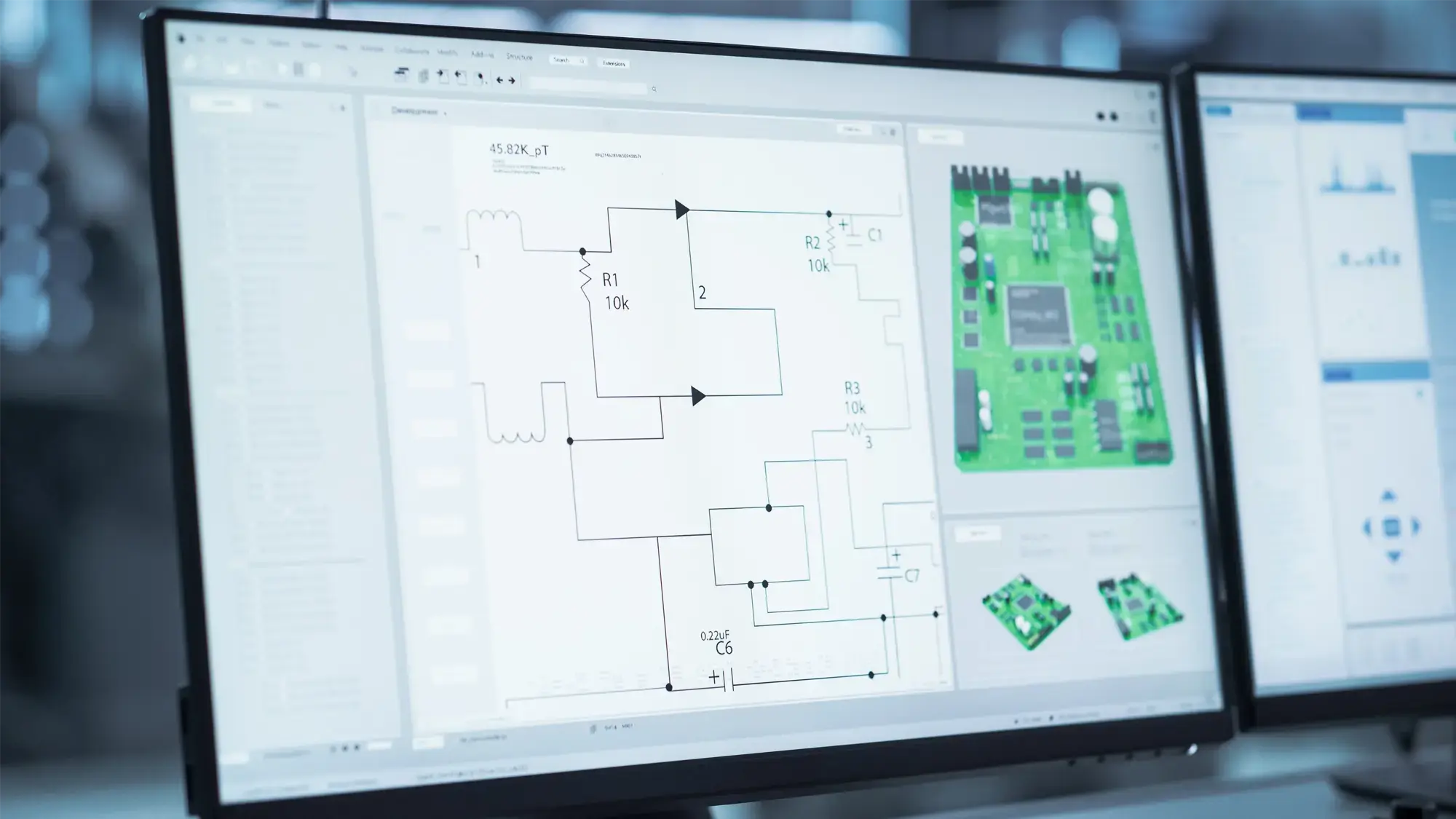
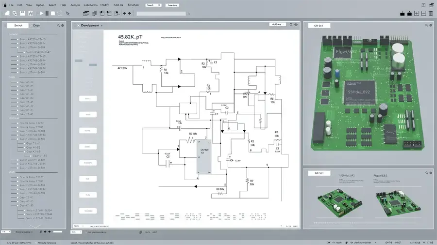
Schematic Capture
We will help you build a well-crafted schematic that ensures high reliability. We accept schematics in multiple formats and convert them into your preferred CAD format.
Our schematic design support includes:
-
Functionality Analysis
-
Power Consumption Analysis
-
Component Selection
-
Symbol Generation
-
Schematic Net Connection
-
Netlist Validation
-
BOM Generation
-
Component Avalibilty Analysis
New
-
Schematic Entry
-
Schematic Validation
Reverse Engineering
Have a critical product that stopped operating due to faulty boards and outdated components? And you lost access to the original design data and documentation? Don’t worry we will bring them back to life.
What we need from you:
-
Schematics Files
-
Old PCB Boards
Cost Optimization Support
Want to streamline your production process and reduce cost without compromising on quality? Our experts will review your existing product or design and propose methods for cost reduction.
Our cost optimization support includes:
-
Suggesting Alternate Materials
-
Optimizing Layout to Reduce
-
Board Size
-
Analyzing Trace and Space
-
Reducing the Number of Layers and
-
Laminations
-
Suggesting Alternate Components
PCB Stack-Up Design Support
Our in-house PCB stack-up design team ensures your project starts off right, aligning with your design objectives for signal integrity, power distribution, and thermal management.
Our stack-up design support includes:
-
Layer Estimation
-
Material Selection
-
Prepreg Thickness
-
Trace and Space
Why Get Help for Your PCB Design?

At Sierra Circuits, we've tailored our approach to PCB design support to solve your toughest challenges and deliver unparalleled value.

Along with our knowledgeable layout experts we have dedicated teams for stack-up support, procurement, fabrication, assembly, and advanced testing. They aren't just here to assist—they're here to solve your design problems.

One of our key strengths lies in our comprehensive checklists crafted by experienced design experts to ensure that your designs are flawless and error-free. We have checklists for schematic, layout, footprint, and BOM, as well as a final pre-delivery checklist.

But here's where we truly stand out: Dealing with different vendors for fabrication and assembly often leads to DFA/DFM incompliance, Sierra operates with a single facility for both. This unique setup ensures that your designs are DFM and DFA-qualified, eliminating any potential delays or errors in the final production.
Trusted by Innovators
Engineers at the world’s most innovative companies choose Sierra Circuits for the highest quality PCB design support services, right here in the USA.


Design Success Stories: How Sierra Circuits Transformed Challenges into Solutions
Case Studies
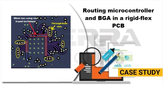
Routing Microcontroller and BGA in Rigid-Flex PCBs
Discover how Sierra Circuits overcame complex challenges to successfully route a microcontroller and BGA in rigid-flex PCBs.
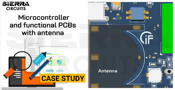
Designing Microcontroller and Functional PCBs with Antenna
The customer is a leading manufacturer of smart home devices that require wireless connectivity and low power consumption.
Softwares We Use Every Day

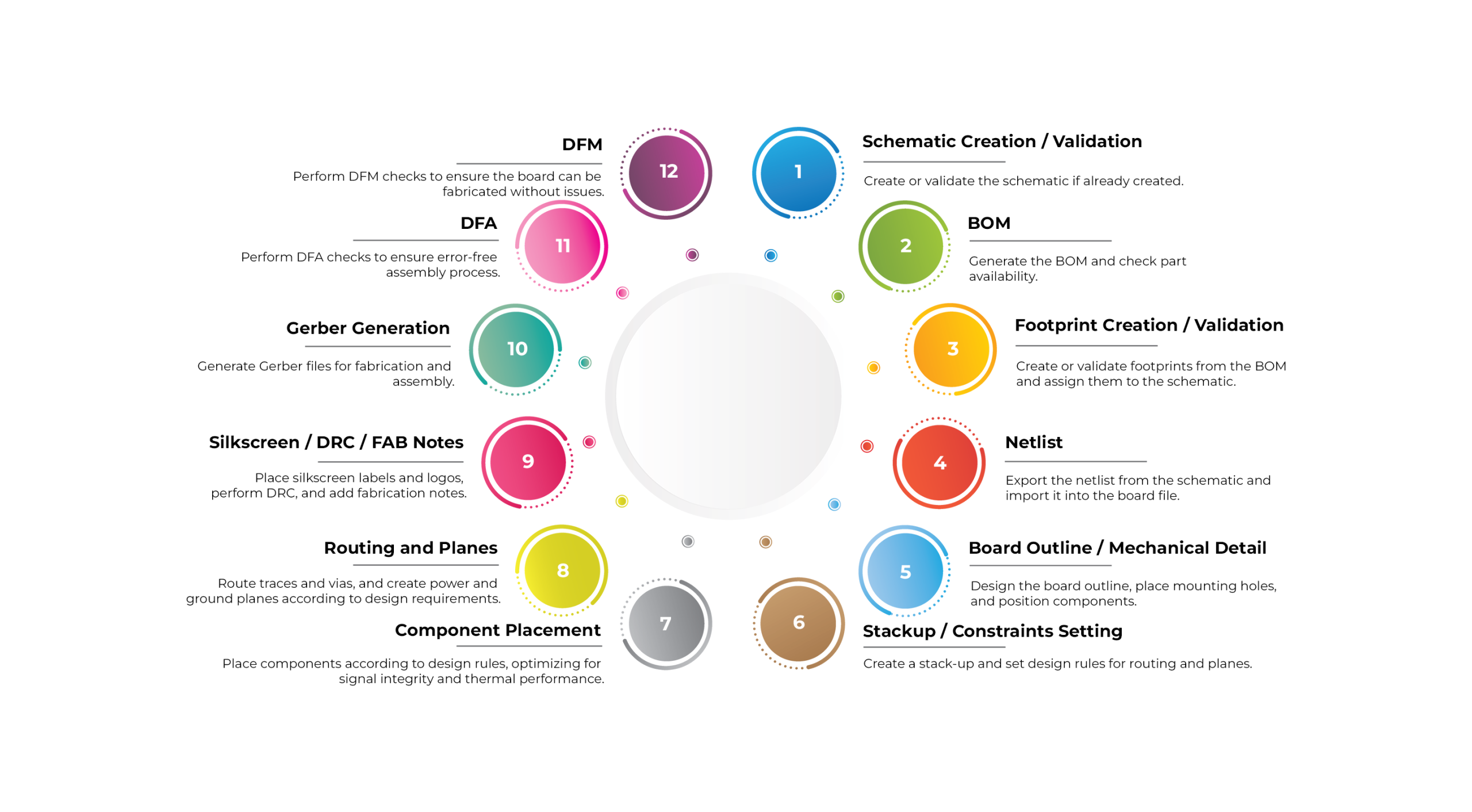
Sierra’s End-to-End Design Support Approach
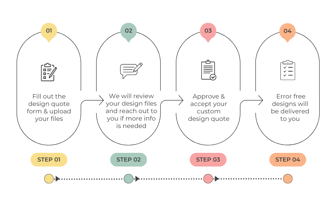
How Does Our Design Support Quote Work?
15 PCB DESIGN TOOLS TO GET YOU STARTED
Sierra Circuits offers online PCB tools for designers to calculate different PCB-related parameters. From impedance and trace width calculation to material selection and stack-up design, designers have a variety of assets to improve their workflow and design precision.


