


Contents

On-demand webinar
How Good is My Shield? An Introduction to Transfer Impedance and Shielding Effectiveness
by Karen Burnham
DFM for HDI PCBs plays a crucial role as they feature fine traces, microvias, and thin dielectrics. Even a minor oversight can cause major fabrication mishaps. Following the design for manufacturing rules ensures your layouts align with the fabricator’s capabilities, minimizing defects, improving yield, and reducing re-spins.
Highlights:
When designing high-density boards:
- Prefer staggered vias over stacked vias to eliminate the need for planarization.
- Maintain annular rings ≥0.05 mm to prevent thermal, mechanical, or environmental failures.
- Select ENIG or ENEPIG surface finishes to improve fine-pitch solderability and mechanical strength.
- Maintain an aspect ratio of 0.8:1 for blind vias.
In this article, you’ll learn the key challenges fabricators face when building HDI PCBs and the critical DFM considerations that help you ensure error-free production.
Why is DFM critical for reliable HDI PCB manufacturing?
DFM aims to identify and resolve potential manufacturing issues in your PCB design before production begins.
Before fabrication, the manufacturer will run a set of design for manufacturing checks to confirm that the production files (Gerber, ODB++, IPC-2581) do not violate the manufacturing constraints, such as trace-to-trace distance, via diameter, and annular ring size.
Without a DFM check, design flaws or manufacturing limitations may surface during production or testing. This can lead to wasted materials, increased costs, and delays.
In HDI PCBs, DFM becomes even more critical because of their unique design challenges, such as:
- Space constraints due to the increasing number of signals, component density, number of pins, etc., limit the space available for routing the traces.
- Complex routing as the available space between pads decreases.
- Tight stack-up registration requirements raise fabrication cost and lower yield.
- Limited options for the use of standard techniques because of the small component footprint and pitch.
To learn how to design reliable HDI PCBs, download our eBook.

HDI PCB Design Guide
5 Chapters - 52 Pages - 60 Minute ReadWhat's Inside:
- Planning your stack-up and microvia structure
- Choosing the right materials
- Signal integrity and controlled impedance in HDI
- Manufacturing considerations for higher yields
Download Now
3 challenges fabricators face in building HDI boards
HDI PCBs integrate more functionality into smaller spaces by using reduced trace widths, smaller via diameters, and lower aspect ratios. Building such fine-feature boards demands extreme precision, making the manufacturing process more complex and challenging. Here, we will see the common challenges in fabricating HDI PCBs.
1. Achieving desired trace width and spacing
To obtain the desired trace width and spacing, manufacturers must maintain high imaging resolution and ensure precise registration. They also need to control etch uniformity to prevent undercuts and distortions. In addition, they should work in contamination-free environments to protect fine-line features.
Some common hurdles in maintaining the desired line width and spacing include:
1.1. Inadequate image resolution and layer misalignment risk fine trace accuracy
Image resolution determines how sharply features are defined during exposure to light, and higher resolution allows finer details to be captured accurately. Similarly, precise layer alignment is essential. Any misalignment can shift copper features, causing shorts, opens, or unreliable connections during manufacturing.
To solve these issues, PCB manufacturers opt for laser direct imaging (LDI). This technique uses a computer-controlled laser beam for imaging. The laser is a highly collimated light source that provides excellent resolution, and the machine aligns each panel individually to obtain tight registration.
It accommodates dimensional changes for a precise image pattern. Additionally, the high photon density improves resist curing while minimizing etchant seepage.
 machine")
Read the case study on designing an HDI board with 0.4 and 0.65mm BGAs to know how we overcame the challenges of placing multiple BGAs in an HDI board.
1.2. Inaccurate trace etching causes undercuts
During the chemical etching process, traces tend to form trapezoidal profiles instead of the desired rectangular shape. This condition is known as an undercut.
The thickness of the copper affects the time required to etch down the substrate. The thicker the copper, the larger the underetch.
To overcome this risk, fabricators often use thin copper weights such as ½ oz, ⅓ oz, or ¼ oz, which helps minimize the undercut to a suitable level.


1.3. Risk of contamination affects trace integrity
Contamination is an important attribute to consider during DFM for HDI PCBs. As trace widths decrease, the probability of contamination due to foreign objects such as dust or hair tends to increase significantly. When the width reduces to 1 mil, even minute contaminants can obstruct a trace, creating voids or causing it to break entirely.
To mitigate this effect, the fabricators must use a class 100 cleanroom as defined by the ISO 14644-1. Cleanrooms are enclosed spaces designed to reduce contamination and control other environmental factors, such as temperature, humidity, and pressure. However, it increases the cost and lead time of the boards.
For more, see why we perform PCB ionic contamination analysis.
2. Drilling vias with a diameter of less than 6 mil
Reduced via sizes can be achieved either by using smaller drills or by decreasing the width of the annular ring.
As a PCB designer, you can focus on reducing via diameters to enhance routing density. At the same time, you should keep your fabricator’s DFM guidelines for HDI PCBs in mind.
Board thickness determines how small vias can be. For thicker boards (typically above 1.6 mm), via diameters generally exceed 6 mil. According to IPC class 3 standards, vias should have a minimum diameter of 8 mil and an annular ring width of at least 4 mil to avoid breakouts.
Lower via sizes bring several manufacturing challenges. They include:
2.1. Mechanical drilling isn’t suitable for producing microvias <6 mil
Smaller via diameters can be achieved through mechanical drilling. But when the via diameter falls below 6 mil, the drill bit loses the strength to withstand the cutting forces. In such cases, laser drilling is preferred.
In HDI designs, microvias require precise controlled depth drilling. Such precision is only possible with lasers.

The size of the microvias depends on the thickness of the dielectric in which the microvias are implemented. Typically, the drill size should be approximately 1.3 times the dielectric thickness. For example, a 3-mil dielectric would require a drill size of about 3.9 to 4 mil.
Despite its advantages, this process has certain obstacles, like aspect ratio constraint, the thickness of the dielectric, and material compatibility.
For laminate selection tips, see how to choose the right HDI PCB materials.
2.2. High aspect ratio restricts reliable copper plating in microvias
The aspect ratio defines how effectively copper can be plated inside holes (vias).
As via diameters shrink and depths increase, plating the interior surfaces becomes more difficult. Achieving reliable copper deposition requires a plating bath with a higher throwing power to ensure the liquid can gush into the minute holes.
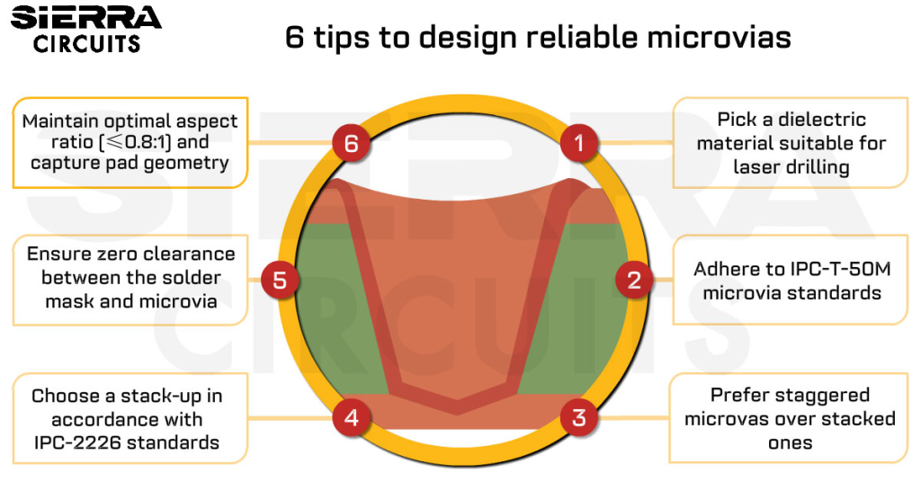
Microvias typically have an aspect ratio of 0.8:1. When the via diameter is about 2 mil, plating becomes unreliable, making aspect ratio one of the most critical considerations in DFM for HDI boards.

2.3. Non-uniform dielectric material reduces hole quality
The dielectric material plays a critical role in determining hole quality and must be suitable for laser drilling.
The procedure of removing material from a surface using a laser beam is called laser ablation. During this process, the resin (FR-4) and reinforcement weave ablate at different rates, which can lead to uneven removal of material and poor hole quality during the laser drilling.
To address this, you need to select materials with uniform thickness. Some manufacturers customize the dielectric to reduce the spacing between weave fibers to achieve more consistent cross-sections. Alternatively, non-woven reinforcement materials such as PTFE or aramid fiber can be used to improve drilling consistency.

2.4. Thin dielectrics increase thermal sensitivity
To maintain the proper aspect ratio, the material thickness should be reduced. Use of standard prepregs or core materials reduces material thickness, but restricts the lower limits for thin standard material. Reinforced materials obstruct further reduction.
The standard board materials are made of epoxy resin with reinforcing fibers. The effectiveness of the reinforcement decreases as the material becomes thinner. It poses challenges as the thickness of the dielectric drops to 3 mil.
When very thin materials are required, non-reinforced dielectrics with thicknesses as low as 1 mil are good alternatives. Some potential options include epoxy liquid, polyimide, and resin-coated copper (RCC).
However, these materials are more sensitive to thermal deviations because their coefficient of thermal expansion (CTE) is lower than that of reinforced materials. As a result, thermal variations must be carefully minimized during manufacturing.

2.5. Via-in-pad increases manufacturing complexities
Microvias can be connected to traces using dogbone or via-in-pad routing. Dogbone routing involves placing a via offset from the pad and connecting it with a minimum-length trace. It loses effectiveness with the decreasing pad pitch. As a result, routing flexibility is limited since the trace and vias block the outer layers.

Vias-in-pad allow immediate signal escape because they are placed inside component pads. As a result, the escape trace is removed, and more space is available for routing. It is the best way for routing, but it still has its downsides, such as additional cost, long lead-time, etc.
PCB manufacturers should create and fill extra vias, adding new steps to the fabrication process, including drilling additional holes and plating vias with copper. These extra steps can add to the overall cost. Also, vias have to be filled with non-conductive epoxy, which is more expensive and time-consuming.

For ultra-HDI PCB design considerations, see designing and fabricating ultra-HDI PCBs.
3. Establishing reliable layer-to-layer connections
Routing flexibility can be enhanced by designing vias to connect only the required layers in an HDI PCB stack-up. However, reducing via height introduces several challenges in design for manufacturing for HDI boards.
3.1. Blind vias are limited by aspect ratio
A blind via connects external layers of a PCB to selected internal layers without passing through the entire board. These vias can be created either mechanically or using laser drilling. Through-hole vias are not feasible since they extend through the whole circuit board.
Blind vias are subject to aspect ratio limitations. Typically, a blind via can connect up to three outer layers. Their reliability is also influenced by lamination cycles, which are constrained by the via structure.
In HDI designs, usually three lamination cycles are achievable; exceeding this can lead to manufacturing issues. You must carefully plan the via structure to manage these cycles effectively.
An alternative approach is the use of buried vias created through a sequential build-up process. This method offers the greatest flexibility for routing, allowing connections between internal layers without impacting external layers, and is often preferred for complex HDI boards.

Always get your fabricator’s approval for your stack-up, and aim for a symmetrical design. Designs with an odd number of layers require extra care during fabrication to avoid potential issues.
Sierra Circuits fabricates and assembles high-density interconnect PCBs with blind, buried, and microvias built across multiple lamination cycles.
Visit HDI PCB capabilities to learn more.
3.2. Stacked vias increase the risk of voids
Connecting multiple layers in HDI boards is a challenging task. Vias can be arranged in either a stacked or staggered configuration to achieve long inter-layer connections. Due to the small size of stacked vias, voids can form while drilling. However, staggered vias will solve this issue.
For more, read design and manufacture of staggered and stacked vias in PCBs.
Using any layer interconnect structure is the most advanced approach in HDI technology. It relies solely on microvias created through a sequential build-up process, providing maximum flexibility in via depth, layer connectivity, and routing options.

Download our eBook for design for manufacturing guidelines.

Design for Manufacturing Handbook
11 Chapters - 96 Pages - 90 Minute ReadWhat's Inside:
- Annular rings: avoid drill breakouts
- Vias: optimize your design
- Trace width and space: follow the best practices
- Solder mask and silkscreen: get the must-knows
Download Now
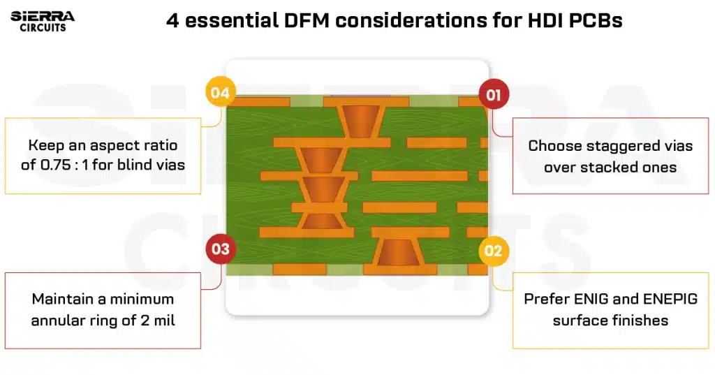
4 essential HDI PCBs DFM considerations
Designing high-density boards requires careful attention to manufacturing constraints to ensure reliability and cost-effectiveness. This section highlights key DFM guidelines for HDI PCBs that help you make informed decisions on via structures, surface finishes, annular ring sizes, and aspect ratios.
1. Choose staggered vias over stacked vias to reduce cost and complexity
Stacked vias require filling and planarization to ensure structural integrity. This process is time-consuming and adds to the overall cost. In comparison, staggered vias eliminate the need for planarization, making them a more efficient and cost-effective option for HDI designs.
Additionally, staggered vias generally provide better mechanical and thermal reliability compared to stacked vias, making them suitable for mission-critical applications such as defense and avionics.
2. Use ENIG and ENEPIG surface finishes for fine-pitch solderability
The right PCB surface finish ensures solderability, planarity, and mechanical strength, which are critical for fine-pitch components in HDI boards.
Here are a few recommendations:
- ENIG: IPC-4552 recommends ENIG for HDI PCBs with BGAs of a very fine pitch because of its planarity and homogeneity.
- ENEPIG: Provides better shear strength for SMT.
Here’s a list of surface finishes offered by Sierra Circuits for HDI boards:
- OSP (Shikoku F2 and Entek)
- ENIG (electroless nickel immersion gold)
- ENEPIG (electroless nickel electroless palladium immersion gold)
- Immersion silver
- Tin nickel
- Electrolytic soft gold
- Electrolytic hard gold
3. Maintain a minimum annular ring of 2 mil for microvias to prevent mechanical failures
Maintaining optimum annular ring dimensions prevents thermal, mechanical, and environmental failures, especially in defense and avionics applications.
Stick to these DFM guidelines for designing annular rings for HDI PCBs:
- The annular ring size should be at least 0.05 mm (2 mil).
- For external layers, a minimum of 20% reduction is permitted in the isolated area caused by defects.
- For internal layers, a 25 μm (1 mil) reduction in isolated areas caused by pits, nicks, pinholes, or dents is permissible.

4. Keep an aspect ratio of 0.8:1 for blind vias
The via aspect ratio (AR) determines the ability to achieve consistent copper plating inside the via. Larger aspect ratios make plating more difficult, increase manufacturing time and cost, and reduce overall PCB reliability. Smaller aspect ratios improve plating quality and long-term performance, especially in HDI designs.
The ideal aspect ratio is 10:1 for through-holes.
AR (Through-Hole) = [(Thickness of the PCB) / (Smallest drilled hole)]
For microvias, the aspect ratio should be limited to 0.8:1.
AR (Microvias) = [(Drill Depth) / (Smallest drilled hole)]
3 design tips every HDI PCB engineer should know
1. Choose materials with Tg ≥200°C for thermal reliability
Selecting the right material is the first step in ensuring HDI PCBs can withstand extreme temperatures, mechanical stress, and electrical demands in defense and avionics systems.
Here are a few considerations:
- Choose materials with a glass transition temperature (Tg) of 200°C and above.
- Select a material that can work above the Tg but below the decomposition temperature (Td).
- Pick a material with a low dielectric constant (Dk) value.
- Opt for a material with high thermal conductivity.
- Pick vibration, shock, humidity, and radiation-resistant laminate.
- Ensure selected substrates are compatible with laser drilling, which enables precise fabrication of blind, buried, and microvias while minimizing defects like carbonization. It can drill a hole of a minimum diameter of 4 mil with precision.
| Material category | Name of board material |
|---|---|
| FR-4 lead-free |
|
| Ceramic |
|
| High-speed RF / MW applications |
|
| Polyamide |
|
| Teflon |
|
2. Ensure your fabricator incorporates positive etchback for reliable connections
In negative etchback, a protective layer is applied selectively before etching away the exposed copper. However, it is not suitable for military and aerospace applications, as the connection established is not strong enough.
In positive etchback, copper is applied and selectively etched. It provides a reliable three-point connection as shown below.
Include the etchback requirements in your fab notes. Here’s how you can call out for positive etchback in your fab notes.
Apply positive etchback as per IPC-6012 class 3. The copper land protrusion must be visible post-desmear.

3. Adhere to class 3 industry standards
Class 3 HDI boards are designed for applications where maximum reliability and performance are critical, such as aerospace, defense, and mission-critical electronics. There are several compliance standards related to defense and avionics that have to be met to satisfy the conformance criteria.
- IPC class 3/A: Military and avionics standard
- AS9100D: Quality management standard for the aerospace industry
- MIL-PRF-55110: Military performance specification for rigid PCBs
- MIL-PRF-31032: Military standard for performance and conformance requirements
- MIL-PRF-50884: Military standard for flexible or rigid-flex board
Sierra Circuits is a MIL-PRF-55110 and MIL-PRF-31032 certified manufacturer, fully compliant with stringent military standards and documentation requirements. See our aerospace and defense PCB manufacturing capabilities to learn more.
The following are the documents provided by Sierra Circuits:
- Certificate of conformance
- Material specifications
- Reflow profile copy (included with first article)
- Photo requirements
- First article inspection report
- IPC J-STD-001E
- Record of calibrated tools used during manufacturing
- AOI report or visual inspection report
- Flying probe or in-circuit test report
- Ionic cleanliness test report
Key takeaways:
- Design for manufacturability ensures PCB design layouts are optimized to reduce fabrication and assembly errors.
- HDI PCBs have unique challenges, such as high component density, limited routing space, complex trace routing, and tight layer stack-up registration.
- Achieving precise trace widths requires high imaging resolution and accurate registration to prevent shorts, opens, or misaligned features.
- Laser direct imaging enables fine-feature accuracy and better resist curing, reducing etchant seepage.
- Etching undercuts occur in narrow traces; using thin copper weights or etching standard copper to the desired thickness mitigates this.
- Contamination risk increases as trace widths decrease; class 100 cleanroom conditions reduce particulate contamination.
- Laser drilling is preferred for microvias <6 mil and ensures precise depth control.
- Compliance with IPC Class 3/A, AS9100D, MIL-PRF-55110, MIL-PRF-31032, and MIL-PRF-50884 is essential for military and aerospace applications.
Following DFM guidelines for HDI PCBs ensures an efficient layout with optimized routing and zero manufacturing defects. Using the right materials, surface finishes, and design features enhances performance.
Need assistance in designing your HDI PCB? Post your queries on our forum, SierraConnect, and our experts will answer them.

About Pooja Mitra : Pooja Mitra is an electronics and communication engineer. With an experience of over three years in the PCB industry, she creates industry-focused articles that help electrical and PCB layout engineers.


Start the discussion at sierraconnect.protoexpress.com