


Contents
BGA technology makes it possible to achieve a smaller form factor in PCBs. With a higher pin count, excellent thermal compatibility, and improved current distribution, they are well-adapted to microprocessors, microcontrollers, RAM devices, and display boards. The smaller the pitch of a BGA, the more challenging it is to break out and route the pins. Some of the challenges that we faced while designing this HDI board with 0.4 and 0.65 mm BGAs are explained in this case study.
We will go over the requirements, the key design limitations, and the methods we used to make the board successful.
Highlights:
- Designing a 16-layer HDI board with 0.4 and 0.65 mm BGAs.
- Stack-up design with a 4-lamination cycle and strategic via connections between layers.
- Overcoming ground connection challenges using via-in-pad structures for larger pitch BGAs and through-hole vias for smaller pitch BGAs.
- Use of stitching capacitors, proper length matching, and serpentine traces for high-speed signals.
- Placement of power-supply bypass capacitors to achieve signal integrity.

HDI PCB design specs with 0.4 and 0.65 mm BGAs
- This is a 16-layer board with an outline of 254mm X 190.5mm.
- The main board is connected to four daughter boards using connectors. The outputs are tested and measured using these sub-boards.
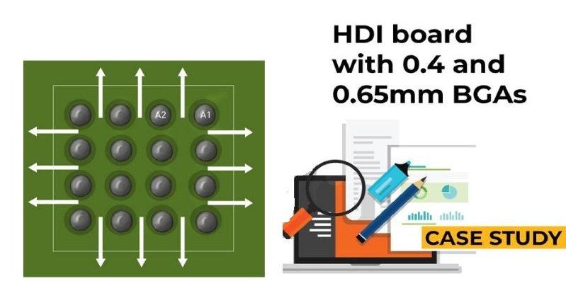
- Three 0.65mm BGAs surround a 0.4mm pitch BGA placed at the center of the main board.
- Sockets are used to mount the BGAs on the board firmly. This requires a clearance of 150 mil from the outline of the sockets.
- Power planes are located between layers 4 and 13.

- The operating frequency of the board is 2.5 GHz.
- A minimum 3W clearance and 135° trace bends were used for high-speed differential signals.
- Stitching capacitors were added close to the vias that connect reference planes to avoid plane obstructions.
- To reduce channel-to-channel skew and prevent stubs, the design incorporates proper length matching of the traces.

- It includes 50Ω and 70Ω single-ended traces and 100Ω differential pairs.
- To make the board suitable for high-speed applications, Isola I-speed material was implemented.
- To avoid the formation of extra resistance between the input pins, the input pins (IN+ and IN-) were connected to the sensing resistor using a Kelvin connection or a 4-wire connection.
- The power-supply bypass capacitor is placed as close as possible to the supply and ground pins to ensure signal integrity.
- Using the JEDEC test, the maximum permitted power dissipation was found to be 2667 mW at 70°C ambient temperature and 150°C maximum junction temperature.
- Blind vias are present between layers 1 and 2, as well as layers 15 and 16. Layers 2-3, 3-4, 4-5, 12-13, 13-14, 14-15, and 4-13 all contain buried vias.

- Due to space limitations, all the blind and buried vias from layers 1 to 5 and from 12 to 16 were stacked.
- The minimum annular ring is 5 mil and 3 mil for mechanical via and microvia, respectively.
- The minimum clearance between the BGAs should be 39 mil
- The minimum spacing between the discrete components is 0.25mm
- The number of lamination cycles is 4
- The BGA pin information is provided below:
| Type of the pin | BGA with 0.4 mm pitch | BGA with 0.65 mm pitch |
|---|---|---|
| Signal | 216 | 90 |
| Ground | 93 | 28 |
| Power | 74 | 150 |

HDI PCB Design Guide
5 Chapters - 52 Pages - 60 Minute ReadWhat's Inside:
- Planning your stack-up and microvia structure
- Choosing the right materials
- Signal integrity and controlled impedance in HDI
- Manufacturing considerations for higher yields
Download Now
Critical design constraints and solutions
Challenges in optimizing the board outline
It is necessary to incorporate the main board and its four daughter boards within a small board area. Through trial and error method, our PCB designers optimized the placement of the three 0.65mm BGAs and achieved the desired dimensions of the circuit board. Initially, these BGAs were placed on one side of the 0.4mm BGA to reduce the board outline. However, that violates the maximum trace width requirement of 53.34 mm (2.1″) between each BGA.
To overcome the hurdle, we decided to place the 0.65mm BGAs around the 0.4mm (center BGA) as shown in the image below.
Issues faced during the stack-up design
The center BGA has 21✕21 pins. Eight of them are dummies, and the rest are signal pins. Since the number of signal pins is high, our design experts first decided to have 5 lamination cycles. However, we did not execute this as it impacted the overall cost of the board.
We decided to have a 4-lamination cycle stack-up with the vias connecting the layers 1-2, 2-3, 3-4, and 4-13.
Design obstacles faced in ground connection
To achieve a proper return path through the center of the BGAs, via-in-pad structures were used for 0.65mm devices. This technique is not feasible for the 0.4mm package due to the smaller pitch size. To overcome this challenge, through-hole vias were added around this BGA for ground connections.

Design for Manufacturing Handbook
11 Chapters - 96 Pages - 90 Minute ReadWhat's Inside:
- Annular rings: avoid drill breakouts
- Vias: optimize your design
- Trace width and space: follow the best practices
- Solder mask and silkscreen: get the must-knows
Download Now
Sierra Circuits’ design team initially analyzes the trace width specifications, regulated impedance, routing density, grounding techniques, and operating frequency of the design.
DFM engineers examine the essential criteria for HDI and high-speed circuit boards to meet manufacturing regulations. By applying the appropriate design techniques, we overcome the difficulties associated with building a complex board. Please feel free to post if you require any assistance with your layout design. Our design experts will be happy to help you.

About Poulomi Ghosh : Poulomi is a microwave engineer specializing in EMI, EMC, RF, and high-speed electronics. As a senior technical writer at Sierra Circuits, she creates advanced engineering articles and webinars for hardware engineers and PCB designers.


Start the discussion at sierraconnect.protoexpress.com