Contents
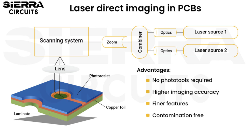
Laser direct imaging (LDI) uses a computer-controlled laser beam to directly define circuit paths onto the board. When manufacturing a circuit board, one of the most critical aspects is printing and etching the layout on the copper-clad laminates.
The imaging process is central to creating a PCB layout and defines the circuit traces. While the conventional imaging process needs a photo-tool film and UV light to transfer the images, LDI improves precision by eliminating intermediate tools and reducing distortion during pattern transfer.
Highlights:
- LDI eliminates the need for phototools, reducing defects and handling costs.
- Improved alignment accuracy makes laser-direct imaging ideal for HDI and multilayer PCBs.
- Photolithography is cost-effective for high-volume production but less precise.
- Environmental factors like humidity and temperature impact phototools significantly.
- LDI offers better control over trace width and registration accuracy.
What is laser direct imaging?
LDI is a printed board patterning process that uses a laser to directly transfer digital circuit images onto a photoresist-coated substrate using a laser, eliminating the need for phototools. It represents an advanced stage in the evolution of circuit board photolithography, offering higher accuracy and flexibility.
Photoresist is selectively exposed to the laser beam in increments across the substrate in a rastering manner. The image formed can be compared to the image on a CRT screen, formed from several lines across the screen.
Similar to photolithography, LDI requires a photoresist, although the resist is specially created for laser printing, as the resist is fast-acting compared to conventional photoresist. The resist comes in dry film and liquid options, with the resist application methods being identical to those used in photolithography.

What are the steps involved in the LDI process?

The LDI follows a sequence of surface preparation, resist coating, digital exposure, and etching. Each step ensures precise pattern transfer and minimal variation, which is critical for high-density circuit designs.
Here’s the procedure:
1. Scrubbing: This includes removing any oxide layers on the core surface using anti-oxidant baths and mechanical scrubbing with abrasive pads. Sometimes Isopropyl alcohol is used to remove any organic residues and oil on the core surface.
2. Lamination photoresist: The board panel is coated with a layer of photosensitive material.
3. Loading CAM files: CAM files are then loaded into the laser.
4. Laser printing: The circuit pattern is printed onto the board by the CNC laser.
5. Etching: Areas of photoresist material that weren’t exposed to the laser beam are etched away using acid, leaving behind the desired circuit paths/traces.
6. Photoresist strip: Removal of the photosensitive material
7. Drying: Drying the core/CCL after removal of photo material
To learn how to communicate your requirements to your CM, download the PCB Fab & Assembly Notes for Designers.

PCB Fab and Assembly Notes for Designers
8 Chapters - 72 Pages - 70 Minute ReadWhat's Inside:
- Guidance on how to write comprehensive fab documentation
- Advanced fabrication notes for flex, rigid-flex, and hybrid stack-ups
- Difference between fabrication and assembly notes
- Assembly documentation essentials: BOM, X-Y data, and drawings
Download Now
Why is LDI preferred over conventional photolithography?
LDI is preferred because it eliminates the need for phototools, improving accuracy and enabling finer features required for HDI PCB fabrication.
Given below are the reasons why laser direct imaging is favored over conventional photolithography:
- Laser direct imaging eliminates the costs associated with the photo tool storage and preservation, along with tracking and continuous inspection.
- A photofilm can be contaminated by dirt, fibers, smears, and scratches, which can degrade the quality and decrease the effectiveness of creating the required circuit pattern.
- A phototool is also affected by the diffraction of light even under ideal conditions. They are also influenced by temperature and humidity variations that can end up distorting the original image.
- There are greater limitations in phototool alignment with regard to the substrate. Flexible circuit substrates may undergo dimensional changes when subjected to processing. In this case, a static phototool can be used to achieve a “best fit”, whereas in LDI the image pattern is precisely adjusted through the computer software for an exact fit, accommodating the dimensional changes. This is important for multilayer circuit fabrication, where printing of traces, vias, and other features is critical.

How does LDI improve layer registration accuracy?
LDI achieves precise layer alignment using laser-based registration instead of mechanical tooling holes. This allows near-perfect alignment and reduces cumulative errors, which is critical in multilayer and fine-pitch designs.
In laser direct imaging, the patterns of the Gerber file are directly exposed to the photoresist film and the laser beam. This creates a sharp image of the circuit. The layer registration is conducted with the help of colliding laser beams from the top and bottom sides of the board.
In this method, there will always be zero-zero registration, which means the beams are perfectly aligned. Now, depending on the flatness of the board, the variations can be up to 5 microns.
Under the traditional photolithography imaging process, films are implemented in photo tools. Films have a glass tray where the tooling holes are distributed, and the same tooling holes are punched on the films, and the registration takes place. The tooling holes control the top and bottom layers.
Sierra Circuit supports ultra-fine 2-mil traces, ensuring tight tolerances for high-performance circuit designs. See our HDI PCB capabilities to know more.
Let’s compare these two methods:
Quality: The photolithography method results in poor-quality images due to fluctuation in temperature and humidity. Laser imaging results in more precision and consistent imaging as compared to photo methodology. Enhanced resolution, precision positioning, perfect alignment, and image trace widths are factors where LDI surpasses.
Environmental impact: Photolithography involves temperature and humidity-controlled environments, whereas laser direct imaging does not have any environmental impacts on the resulting images.
Variation: In this photolithography registration, when you plot a film from Gerber data, there will be a 5-micron variation. During the transition from the film to the board will be 10–15-micron variations due to board warpage and tooling tolerances.
In total, there will be 15–20-micron variations. In LDI registration, there will be a 5-micron variation depending on the flatness of the board.
| Parameter | Photolithography | LDI |
|---|---|---|
| Quality | Poorer due to environmental variation | Higher precision and consistency |
| Alignment | Tooling hole-based | Laser-based dynamic alignment |
| Variation | 15–20 microns total | ~5 microns depending on flatness |
| Environmental Impact | Sensitive to humidity and temperature | Minimal impact |
How does conventional PCB photolithography work?
Photolithography uses UV light and phototools to transfer circuit patterns onto photoresist. While it is efficient for large-scale production, it is more prone to alignment errors and environmental distortions compared to LDI.
Circuit board fabrication has been dependent on the conventional photolithography process for quite some time. In traditional photolithography, a photographic mask called a phototool is created from a drawing and placed on a panel covered by photoresist.
The photoresist will then be exposed to a UV light source to harden/develop, after which the panel is etched with chemicals to retain the circuit pattern.
While generating the phototool itself is a time-intensive, multistep process, automated exposure systems set with a 5-second exposure time can generate up to 150 panels per hour.

Here is a sequence of steps undertaken in conventional photolithography to print a circuit pattern:
1. Scrubbing: Surface preparation for the cores is done similar to the process mentioned in LDI.
2. Lamination photoresist: Photosensitive film called photoresist is placed on the core surfaces at 75-80 °C to bind it to the core surface. This phase is also called creating a presensitized PCB, as the surface of the circuit board is made sensitive to UV light exposure.
3. Exposing: Exposing the photo material to UV light. It causes a change in the photoresist material, which causes it to harden or become more soluble, depending on whether it is a negative photoresist or a positive photoresist, respectively.
Later, the remaining unhardened photoresist material will be etched away using chemicals.
4. Positive image: When using a positive image, UV light is made to hit the material in the regions where the copper must be removed. Once the positive image is exposed to the UV light, the photoresist becomes more soluble in the photoresist developer solution. This will leave behind an identical copy of the pattern.
5. Negative image: When using a negative image, UV light is made to hit the material in the regions where copper must be retained. The region exposed to UV light polymerizes and hardens, so that the developer solution will wash away the unexposed photoresist regions. This will leave behind an inverse copy of the pattern.
6. Developing: This involves using chemicals to induce reactions in the photosensitive film and cause it to dissolve. Usually, the developer solution is a 1% solution of Sodium Carbonate (Na2CO3) or Potassium Carbonate (K2CO3). Both solutions yield similar results, except that Potassium Carbonate is known to give slightly better quality results with regard to developing.
7. Automatic optical inspection (AOI): This involves checking the existing CCL against circuit patterns that are present in the system. The AOI inspection process involves scanning the board surface.
The AOI equipment includes one or more high-definition cameras that capture images of the board surface using several light sources. The images are then compared in real-time with the required board patterns using built-in processing software. The full process can be carefully monitored throughout.
Also read, PCB cross-section analysis: a microscopic visual validation of PCBs
8. Etching: This is a process where unwanted copper on the board is removed. Copper covered under dry film remains. Circuit board manufacturing processes use solvents like ferric chloride, cupric chloride, ammoniacal etchant, sulphuric and chromic acid, alkaline etchants, and copper ammonia complex ion as etching fluids.
9. Photoresist strip: Removal of the photosensitive material
10. Drying: Drying the core/CCL after removal of photo material
Laser direct imaging is the next step in the evolution of the circuit printing process. Even though it is more expensive than conventional photolithography, it is invaluable in the manufacture of high-precision prototype boards. The adoption of LDI in PCB manufacturing is increasing and showing no signs of slowing down.

About Poulomi Ghosh : Poulomi is a microwave engineer specializing in EMI, EMC, RF, and high-speed electronics. As a senior technical writer at Sierra Circuits, she creates advanced engineering articles and webinars for hardware engineers and PCB designers.