


Contents
Incorporating proper PCB grounding techniques, such as dedicated ground planes, ground vias, and galvanic isolation, is critical in building reliable and safe electronic designs. It is even more critical in high-power and high-density boards as they’re prone to unwanted noise, interference, and other electrical hazards.
Grounding methodologies in circuit designs mainly depend on the board’s dimensions, layout requirements, and technology like rigid, flex, and rigid-flex. Managing high currents and voltages in a dense layout with mixed and high-frequency signals is one of the primary challenges. In this article, you will learn some of the efficient grounding strategies that need to be followed in high-power and HDI designs.
Highlights:
- Ground plane provides a common reference point for signals and power, ensuring safety, EMI control, and signal integrity.
- Common ground types include signal, power, virtual, floating, AC, chassis, and protective earth grounds, each with distinct applications.
- Proper PCB grounding techniques, such as dedicated ground planes, ground vias, and galvanic isolation, are essential for reliable electronic designs.
- Ground loops can be prevented using ground traces, multi-point grounding, and proper component-to-plane connections.
What is the purpose of grounding in PCBs?
Ground provides a common return path for signals and power. It also serves as a reference point in a circuit to measure voltages across various points. Efficient grounding is quintessential for the safe operation of a circuit board. A robust ground system provides a solid foundation for a good power delivery network topology. In addition to this, it aids in thermal management, averting EMI, and ensuring signal integrity. See how grounding controls noise and EMI for more.
For better results, you need to adhere to best routing practices that establish reliable connections between the components and ground planes.
Different types of ground in circuit board designs
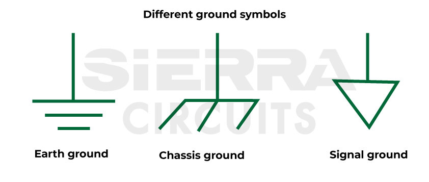
There are various types of grounding, each represented by different symbols. They are:
Signal ground
It is a point on the board from where a signal’s voltage is measured. This reference point will be connected to an internal ground plane. If your design has analog and digital signals, you need to have separate ground paths for each of the signal types.
Power ground
This facilitates a signal return path for power signals. It is typically DC and must be grounded separately from other signals.
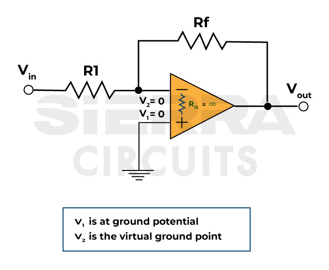
Virtual ground
This type of ground is not connected to a ground plane. An op-amp feedback is an example. In the image below, point V2 is considered virtual ground. This point will not be able to sink infinite current as the input impedance is very high. When the non-inverting input is at zero volts, the negative feedback will hold the inverting terminal at the virtual ground to match it. It is not a stable return for other circuits. Virtual grounds can be used to analyze an op-amp’s functionality.
Floating reference
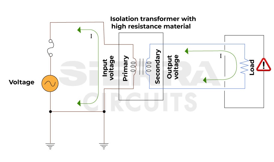
In an isolated system, the floating ground is a large reference conductor that is not physical connection to the earth. Hence, the voltage at the ground terminals and conductors is undetermined. The unintentional floating ground is considered a system fault, though in some cases it is intentionally used for safety.
For example, in the circuit below, isolation transformers are used in low-voltage (LV) power supplies to separate the main ground from the LV reference. The grounding current path from the main supply is avoided by floating the LV ground. Even if there is a fault on the LV side, it provides electrical safety.
AC ground
They are ground paths with low impedance that block DC return currents, normally obtained by connecting a capacitor to a ground plane.
Chassis ground
Here, PCB is connected to a metal chassis body. As a safety measure, this enclosure is directly connected to the earth ground. Additionally, it can have RF filters and ESD protection measures. This system can have parasitic capacitance as shown in the figure.
Protective earth return path
It is a physical connection to the earth that acts as a safe return point for surplus current. It provides a channel to dissipate unwanted energy and protect the circuit, especially in high-voltage power supplies.
RF & Microwave Design Guide
8 Chapters - 44 Pages - 60 Minute ReadWhat's Inside:
- Basics of RF and microwave board design
- Choosing RF materials
- Trace, grounding, via, and stack-up design
- Component selection and placement
- Testing and isolation requirements to avoid interference
Download Now
6 PCB grounding techniques for high-power and HDI designs
The grounding guidelines will be different for isolated and non-isolated power circuits. You can find the best grounding solution for your application using combinations of PCB grounding techniques discussed in this section.
1. Dedicated ground planes
A ground plane is a copper layer in your stack-up that provides an easy signal return path. Generally, this plane is placed right below the signal plane to reduce the return path. They allow controlled impedance signal routing in a microstrip or stripline configuration. Here, one of the interior copper planes is normally dedicated as a ground plane in a multilayer PCB.
Having separate ground planes for high and low-voltage sections can help reduce crosstalk and maintain signal integrity in high-density boards. These ground planes should be connected separately to the power supply. Large ground planes help with the thermal management of higher currents as they act as heat sinks to transport heat evenly throughout the board, preventing high-power PCB failure.
Enhance your board’s thermal performance by implementing expert insights into your design- see PCB heat dissipation techniques by Keven Coates
Follow these guidelines when you have dedicated ground planes in your design:
- Always keep the ground planes uniform without splits. This minimizes the voltage drops and improves signal integrity.
- Place the ground plane below the signal plane to reduce the return path. This helps in reducing conductive rings and ground loops.
- Have separate grounds for input AC, unregulated, and regulated DC sections in power systems for sound electrical isolation.
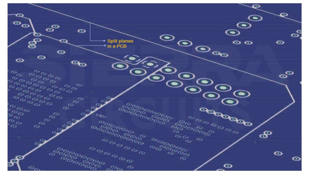
- Split planes must accommodate multiple power or ground nets carefully, as they could inadvertently ruin or block a clear signal return path.
- Route the nets such that they do not intersect to avoid interference.
- Use stitching capacitors when the signal changes its ground reference.
- Use ground fill (copper pour) to achieve uniformity in the ground planes. These are then connected using vias.
- Employ a common ground plane strategy where the free space on a PCB is covered using copper pours.
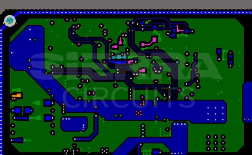
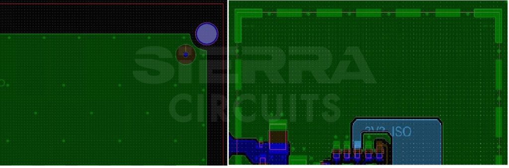
- Keep power planes away from PCB edges as they can cause interference. Instead, employ ground planes (act like a shield) at the board edges even on power planes.
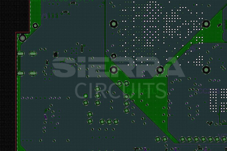
Ground plane polygon (green) at the board edge
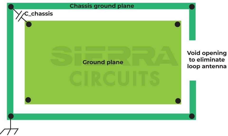
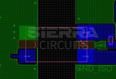
When using a chassis ground, place a void in the ground section connecting to the chassis to eliminate a ground loop antenna. An AC ground point is provided using a capacitor. When the equipment uses wall power to return directly to the earth, this situation is ideal.
The capacitor used for coupling the chassis polygon and normal ground on the PCB is to provide isolation of DC signals and a bypass path for high-frequency noise signals. Select capacitors with low ESR and high voltage ratings. Normally chassis plane is directly shorted to the ground plane if the return current of the circuit is less. In case of very high return current, isolate chassis planes using capacitor connections.
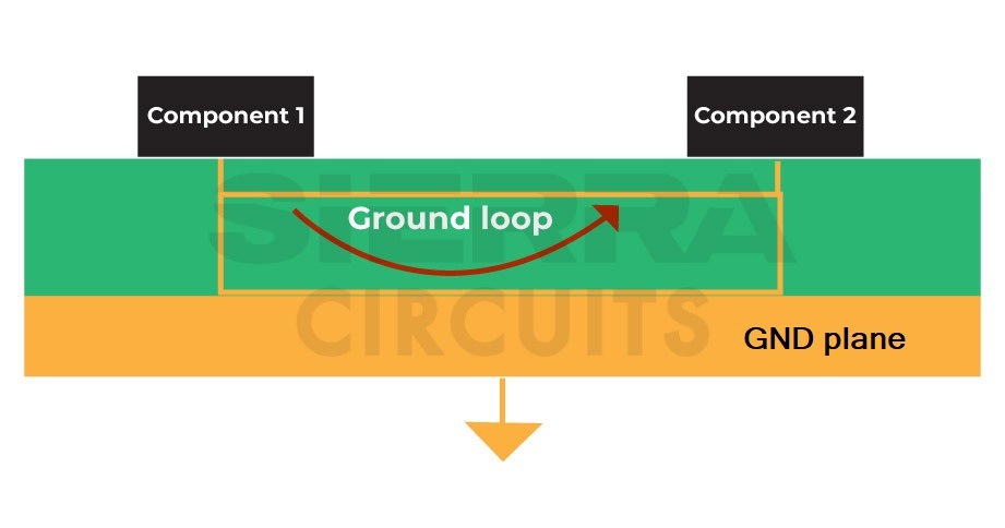
2. Ground traces to prevent ground loop
Ground loops occur due to multiple current return paths caused by the difference in ground potentials throughout the circuit. To keep the same ground voltage throughout the board, the ground pins of connectors and components are connected individually to their respective ground area.
This is done through separate vias or short traces.
This is called multi-point grounding and is mainly used in high-frequency designs.
When you use the multi-point PCB grounding technique, use thermal relief pads for through-hole components that connect to any plane. This ensures that the pad provides enough metal to conduct the current, but will also help conserve heat for easy soldering during assembly.
Do not have sensitive traces (clock and other digital signals) close to the power traces to avoid noise. Internal traces can be narrower than external ones as they are not exposed to outside interference. Always use wide ground traces to prevent overheating and minimize ground impedance in high-current PCBs. In high-voltage boards, maintain adequate creepage and clearances between conductors to prevent arcing.
If there are no exclusive ground planes in your stack-up, you should use the smallest trace width possible for signals (6-8 mil minimum). Keep the power and ground traces about 15-25 mil. However, it is important to understand that the trace width of a conductor is proportional to the current flowing in it.

Guard traces reduce crosstalk
Guard traces are implemented to reduce crosstalk. They are often installed on both sides of a sensitive signal and grounded at both ends.
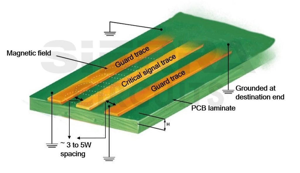
It is not practically possible to have guard traces for HDI boards, as it takes up more space. Prefer not to use them for controlled impedance traces. If used for impedance traces, maintain a minimum of 3W-5W spacing so that it doesn’t affect the impedance.
To get some valuable insights into the HDI PCB routing challenges, read 5 HDI PCB routing challenges with solutions.
3. Galvanic isolation with separate high and low-voltage sections
When you’re working with high voltages, galvanic isolation must be implemented to prevent damaging currents from passing through the operator’s body or to other parts of the circuit. It is also used when two sections of a circuit have different ground potentials and a signal needs to be transferred between them. This avoids the coupling of unwanted AC and DC between the two parts.
You can use this technique to break ground loops to maintain communication integrity. Use transformers (step up/down) along with fuses and capacitors for power isolation. The exchange of information between isolated sections is provided by using optocouplers, hall sensors, or relays.
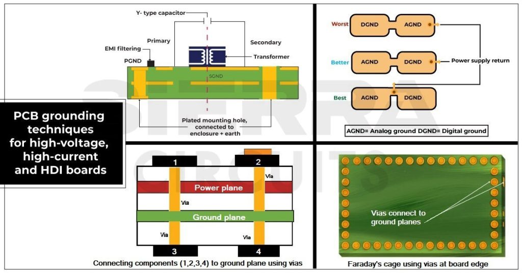
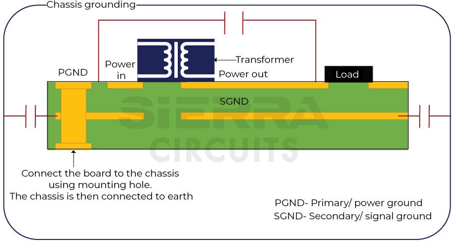
For instance, when your input power is from a 3-wire single-phase AC that carries high currents, a transformer is used to obtain a stepped-down voltage to meet the board’s power needs. The ground connection to the transformer primary is called primary ground (PGND). Ground connected to the transformer secondary and other parts of the PCB is called secondary ground (SGND). This format galvanically isolates the power supply of the board physically.
When you need to preserve DC isolation in a power system, implement galvanic isolation as shown in the figure below. Connect the ground plane to the earth only at the input(primary side). Use plated mounting holes to establish a connection between the chassis and the circuit board. On the output (secondary side), only connect the plated mounting holes to the chassis, but not to the PCB ground.
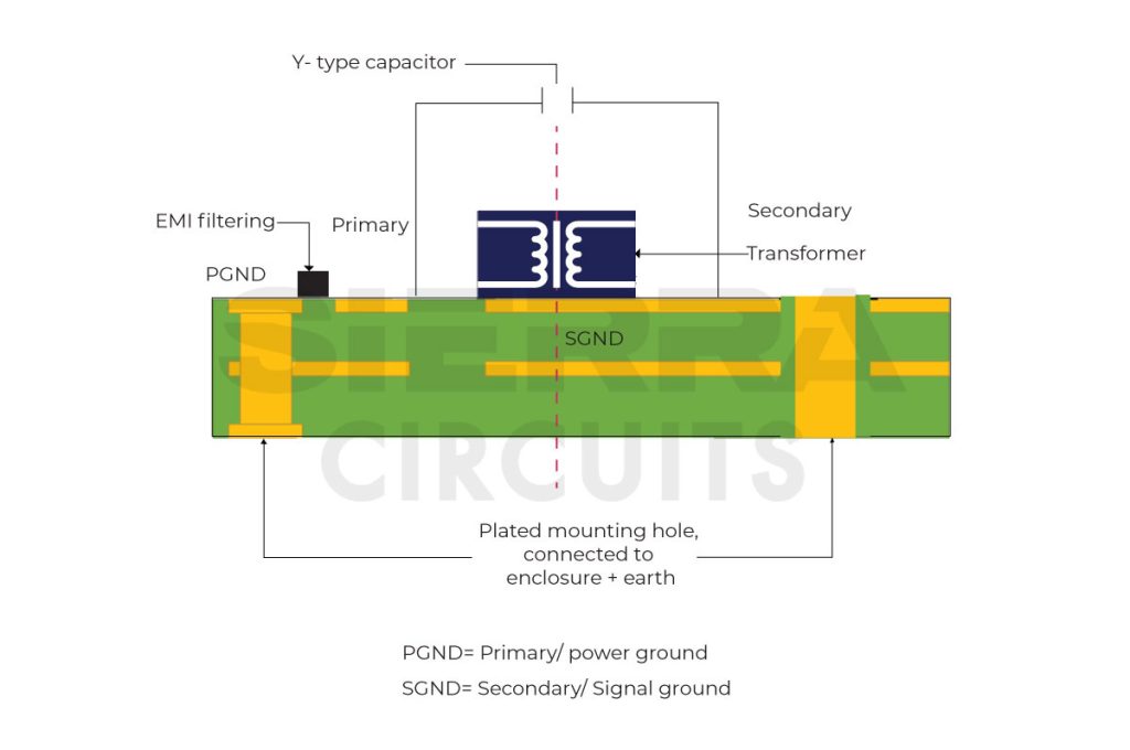
Bridge PGND and SGND with a class Y capacitor to prevent noisy radiated emission. This ensures galvanic isolation for large DC and uniform ground potential for AC. It also prevents a shock at the primary side from reaching the output.An
EMI filter can also be used in the isolated primary input side to direct any low-level noise to the ground. High-frequency differential or common-mode noise from the secondary side can be connected to the earth through the primary side. If an ESD event occurs at the input/output connector, it can be connected to SGND. The same path is then followed to connect to the Earth to prevent any hazards.
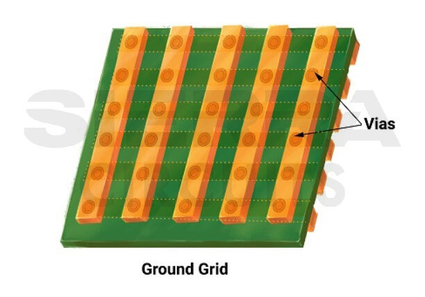
4. Ground plane vias and via stitching
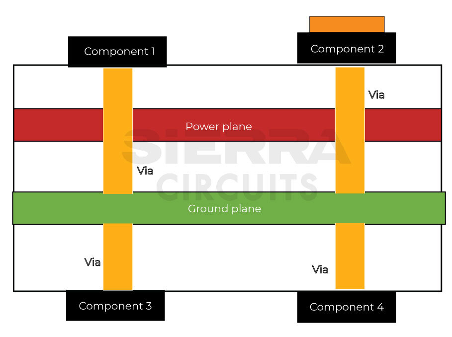
Ground plane vias provide direct access to the ground plane from a point on a board. The idea behind this is to keep the signal return paths short and reduce ground loops. This type of PCB grounding technique is very useful for high-density boards with 4 or more layers.

HDI PCB Design Guide
5 Chapters - 52 Pages - 60 Minute ReadWhat's Inside:
- Planning your stack-up and microvia structure
- Choosing the right materials
- Signal integrity and controlled impedance in HDI
- Manufacturing considerations for higher yields
Download Now
Via stitching is done at specific intervals to ensure shorter ground return paths in the PCB from the load devices to the power source. As a thumb rule, ground vias can be placed at 1/8th of a wavelength or less from the relevant conductor to prevent resonance. Via stitching can also protect critical components from high power, as it can help in heat transfer to a thermal landing. When power planes are close to the board edge, they interfere with other layers. This can be avoided via stitching with 50-100 mil spacing at the edges, as it acts as a shield (Faraday’s cage).
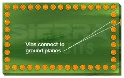
Take care of board edge stability when it comes to the spacing between vias, as it can affect depanelization during assembly and break your board.
Ground grids are to provide suitable reference planes for traces. When there is no possibility of having an entire ground plane due to space constraints, they are laid out with vias at suitable intervals. Ground grid structures are also used in flex boards, where having an entire ground plane can affect flexibility. Find areas where you can provide ground strips with openings to ensure that bendability is maintained. This is called hatching, where the strips are generally at 45° angles.
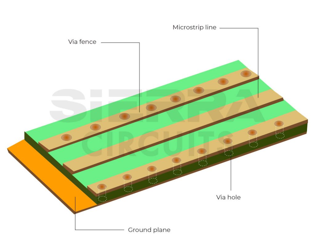
Via fencing technique is used based on special design requirements like RF boards, which contain microstrip lines and coplanar impedance traces. If there is a trace from an RF connector, provide ground strips on either side of the trace with appropriate spacing and via stitching.
5. Place bypass and decoupling capacitors to avoid ground bounce and coupling
When a power rail is distributed and shared between multiple board components, the active components may generate dangerous phenomena, such as ground bounce and ringing.
Ground bounce phenomenon occurs when the voltage of different ground reference points on the board fluctuates. The most common method is to place a bypass capacitor on the circuit, which effectively bypasses the voltage spikes and power supply noises. Place the bypass capacitors close to the power supply pin of each device on the board. Connect them to the ground using short traces or vias separately. Avoid a daisy-chain ground connection as it increases inductance.
Decoupling capacitors are used in parallel to the power supply to decouple the incoming AC signals from the DC signals. These are connected between the power pins and a ground plane. A trace is not ideally used to connect the IC and the capacitor ground. They smooth out oscillations generated by the supply voltage, reducing noise and EMI. They filter out any spikes that occur and protect the different ICs in the circuit. Placing decoupling capacitors close to the power supply pin ensures that the IC receives power irrespective of voltage fluctuations.
Here’s what Syed Ubaid Ali Warsi has to say about high-speed and HDI PCB design considerations.
6. Ground wires and lightning protection devices for safe operation
High-voltage and high-current systems can be made safe by avoiding high leakage currents in printed boards through:
- Using grounding wires to provide a low-impedance path for return currents in high-power boards
- Employing surge and lightning protection devices and methodologies. These devices work by routing away voltage spikes from the electrical components and dispersing them to a ground plane. Here, the ground plane can be a copper pipe inside a building or the earth. Air gap arrestors, gas discharge tubes, and power isolators are devices that are used for ESD protection. Fuses can be used to protect from short circuits, current, and voltage overloads. Select them based on the breaking capacity rating, voltage rating of the system, and packaging.
Need help in designing reliable PCBs? Our engineering team can help you with thermal management, stack-up design, and DFM analysis.
You can book a meeting with our experts or call us at +1 (800) 763-7503.

Key takeaways:
- Select grounding methods based on board type, operating voltage/current, and signal frequency to optimize performance and safety.
- Use continuous, split-free ground planes placed below signal layers for controlled impedance and noise reduction.
- Isolate high- and low-voltage grounds using galvanic isolation to prevent hazardous coupling.
- Incorporate via stitching on board edges at regular intervals to create effective shielding and maintain uniform ground potential.
- Position bypass and decoupling capacitors close to device power pins with short, direct ground connections.
- For high-voltage and high-current boards, implement robust surge and lightning protection systems tied to a reliable earth or chassis ground.
High-voltage, high-current, and HDI boards require a well-structured grounding system to ensure the reliability of the overall system. Without proper grounding, your design can experience EMI and noise. Consider these PCB grounding techniques before routing your next design.
Have questions on your PCB design? Post them on our forum, SierraConnect. Our design experts will answer them.


