


Contents

On-demand webinar
How Good is My Shield? An Introduction to Transfer Impedance and Shielding Effectiveness
by Karen Burnham
PCBs with high operating current and voltage should adhere to specific layout rules to avert overheating and arcing issues. While adequate trace width ensures safe high-current transmission, the right creepage and material with high CTI are vital to designing an efficient high-voltage PCB.
In this case study, you will learn the challenges that we encountered during the design phase of a high-current circuit board and how we successfully resolved the issues. We will explain the strategies that we implemented to allow specific voltages and currents to traverse without causing damage to the circuitry with voltage doublers. Voltage doublers are multiplier circuits that amplify the input voltage by a factor of 2 at the output.
Design specs for this high-current PCB
- The design has 4 layers with a dimension of 16 ✖ 22 inches.
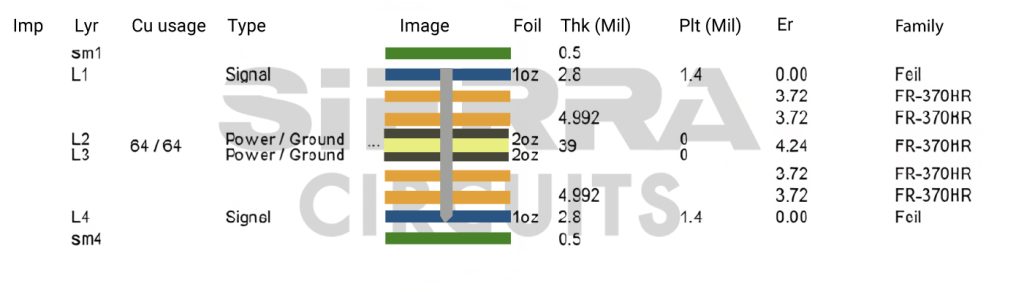
- It incorporates FR-370HR material, which offers a higher Tg of 180 ℃ and good insulation with more than 600V of CTI.
- The circuit requires 230V of voltage and 40A of current at the input.
- The operating frequency is set at 60Hz.
- The board has 2oz of copper thickness.
- The DC voltage doubler circuits are used for the power supply.
- The circuit includes 12 transistors to carry the high current. These transistors act as switches. 24 capacitors present in this design charge up while the transistors are in the off state. When transistors are turned on, capacitors discharge, doubling the voltage at each level. This kind of circuit configuration is known as a charge-pump regulator.
- Conformal coating is used to protect the board from corrosion and to provide electrical insulation for high-voltage circuits.
- The surface finish chosen here is ENIG.

High-Speed PCB Design Guide
8 Chapters - 115 Pages - 150 Minute ReadWhat's Inside:
- Explanations of signal integrity issues
- Understanding transmission lines and controlled impedance
- Selection process of high-speed PCB materials
- High-speed layout guidelines
Download Now
Challenges we faced while designing the high-current board
- The operating voltage requirements are different in three phases: 480 V, 640 V, and 960 V. Each phase includes 8 capacitors and 4 transistors.
- To equate the input and output powers, the initial 40 A current is gradually reduced to 30 A, 20 A, and 10 A as the voltage rises in three phases.
- The board generates an enormous amount of heat as it demands high operating voltage and current within its 4 layers.
To learn how to tackle elevated voltage and current in your power electronics board, see how to select components and materials for power electronics PCBs.
Techniques and tools that helped us design this board
1. We used the PCB Conductor Spacing and Voltage Calculator to determine the right clearance for this high-voltage board.
The table below shows the different conductor spacings we set based on the voltage levels.
| Operating voltage (volt) | Clearance values (mil) | |
|---|---|---|
| Internal layer | External layer with conformal coating |
|
| 230 | 8.6 | 19.8 |
| 480 | 13.6 | 40 |
| 640 | 28 | 56 |
| 960 | 60 | 91.2 |
2. Based on the current, we calculated the conductor widths using our Trace Width Current-Capacity and Temperature Rise Calculator. The following table shows optimum trace widths for different current levels:
| Operating current (A) | Trace width (mil) |
|---|---|
| 10 | 328 |
| 20 | 1094 |
| 30 | 2215 |
| 40 | 3652 |
3. Via stitching was implemented to ensure a low-impedance path and accelerate heat dissipation. Our Via Current Capacity and Temperature Rise Calculator helped to decide the number of vias required to be stitched for individual operating currents. The via count for various operational currents is shown in the table below.
| Operating current (A) | Number of vias to be stitched |
|---|---|
| 10 | 6 |
| 20 | 11 |
| 30 | 16 |
| 40 | 22 |

4. Multiple heatsinks were placed near the high-current-carrying transistors, which generated more heat as compared to other parts of the board. While positioning heatsinks, designers emphasized avoiding airflow obstruction through the board.
5. We ensured sufficient space between reference planes, so that, voltage spikes from one layer would not transit into the next layer.
6. We implemented film capacitors with a low ESR (Equivalent Series Resistance), and low dissipation factors. These capacitors withstand high voltage ranging in KV and carry high-current pulses.
Need help in designing reliable PCBs? Our engineering team can help you with thermal management, stack-up design, and DFM analysis.
You can book a meeting with our experts or call us at +1 (800) 763-7503.

Key takeaways from this case study
- You need to determine the right clearance values to prevent arcing between the conductors.
- Ensure that the traces are wide enough to allow high-current transmission.
- Incorporate via stitching to improve the electrical and thermal performance of your high-current design.
- Install heat sinks next to the parts that produce a lot of heat. Place them carefully so that the airflow through the board is not affected.
During the design phase, we analyzed the circuit requirements and calculated high-voltage clearances, trace widths, and positioned the heat sinks without impacting the airflow through the board. We chose film capacitors and implemented via stitching to create a low-impedance path and aid heat dissipation.
For more efficient PCB heat dissipation techniques, see 12 thermal management techniques to reduce PCB heating.
The engineers at Sierra Circuits have expertise in designing complex high-current, high-voltage, and RF/microwave boards with frequencies from 10 MHz to 30 GHz. If you have any questions about developing boards with high operating current and voltage, please feel free to comment below. Our team will be glad to assist you.

About Poulomi Ghosh : Poulomi is a microwave engineer specializing in EMI, EMC, RF, and high-speed electronics. As a senior technical writer at Sierra Circuits, she creates advanced engineering articles and webinars for hardware engineers and PCB designers.


