Contents

On-demand webinar
How Good is My Shield? An Introduction to Transfer Impedance and Shielding Effectiveness
by Karen Burnham
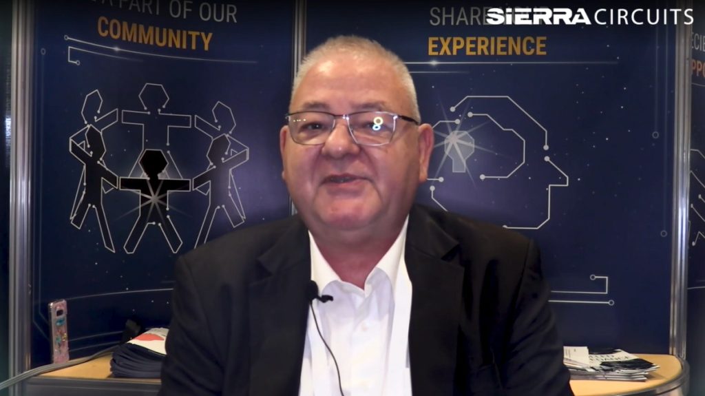
Laurent Nicolet, the Vice President of Business Units Electronics at the Schmid Group, talks about the future of wet and dry PCB etching technologies and machinery in this interview.
Laurent has been in the PCB industry since 1982 and has a unique perspective to share.
Highlights:
- The dry etching method, utilizing plasma technology, is the future of PCB etching.
- It requires ABF with silica fillers or polyamide for base material.
- Vertical machines, equipped with magnetic clamps, facilitate easy transport of panels as thin as 25 microns.
- HDI mSAP approach achieves an impressive line spacing of just 7 microns.
Watch the full video to know more.
What does Schmid do?
Laurent Nicolet: Schmid specializes in creating processing machines for the printed circuit board and photovoltaic industries. Traditionally, its focus has been on wet processing machines. However, in the last five years, in addition to wet processes, the company has ventured into dry PCB processing techniques. Schmid has been actively developing technologies like plasma and sputtering for printed circuit boards, embracing innovation and diversifying its expertise.
What approach would you suggest for transporting flex PCBs through the wet processing machines?
Laurent Nicolet: Our customers often raise a significant concern regarding the transportation of flex PCBs. They’re keen on using roller transport for the thinner boards during wet processing, but this comes with certain limitations. Our roller system can safely handle boards with a maximum thickness of 32 microns. To address thinner boards, we’ve developed a vertical machine equipped with magnetic clamps, allowing us to transport panels as thin as 25 microns with ease.
Flex PCB Design Guide
10 Chapters - 39 Pages - 45 Minute ReadWhat's Inside:
- Calculating the bend radius
- Annular ring and via specifications
- Build your flex stack-up
- Controlled impedance for flex
- The fab and drawing requirements
Download Now
Which processes are most critical for HDI production?
Laurent Nicolet: HDI production is moving from the subtractive method to the mSAP process, which is highly sensitive. A critical component of this process is the photoresist in its initial development phase. Hence, to address this sensitivity, we’ve introduced the InfinityLine V+. This innovative system enables us to transport panels through the vertical line using magnetic clampers, all while avoiding any contact with the active surface. By eliminating direct contact, we’ve improved board yield.
The HDI mSAP approach achieves a remarkable line spacing of 7 microns, therefore making it critical to protect the surface. Hence, our clampers employ a completely touch-free system, ensuring precision and quality in the production process.
Learn more about high-speed HDI designs from another expert. Read high-Speed and HDI PCB design strategies by Syed Ubaid Ali Warsi
HDI PCB Design Guide
5 Chapters - 52 Pages - 60 Minute ReadWhat's Inside:
- Planning your stack-up and microvia structure
- Choosing the right materials
- Signal integrity and controlled impedance in HDI
- Manufacturing considerations for higher yields
Download Now
What plans do you have in store for the future of PCB manufacturing?
Laurent Nicolet: As a machine manufacturer, we constantly aim for innovation and future readiness. Our collaborations with OEM companies have led us to push the boundaries of what’s possible.
We’ve been asked not just to limit the line and space widths down to 10 microns but to space it as narrow as 2 microns.
Therefore, to meet this demand, we have developed an innovative process, exploring the concept of PCB etching the base material to create embedded traces. This cutting-edge approach required the creation of new wet processing machines tailored to handle this groundbreaking design.
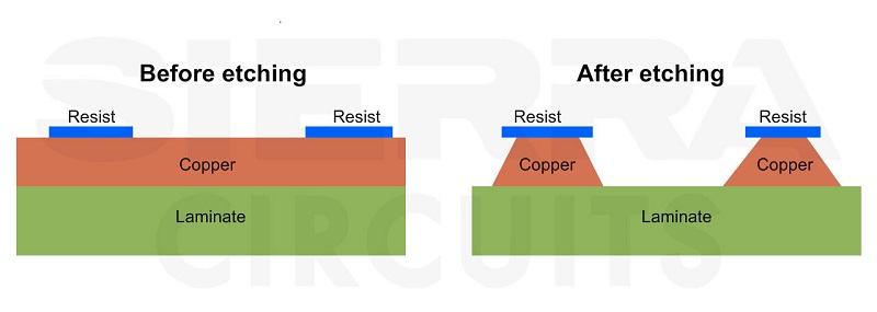
In the process, we introduced a dry method involving plasma technology to etch the base material. We also revolutionized the metallization process by replacing electroless copper with sputtering. This significant change enables us to achieve line and space dimensions as narrow as 2 microns. Importantly, this breakthrough technique is applicable to a range of materials, including HDI, HDI+, and flex materials. However, this process is not compatible with glass fiber materials. Instead, we must use materials like ABF with silica fillers or polyamide to achieve these exceptional results.
Key takeaways:
- Schmid has introduced a future-oriented dry PCB etching process using plasma technology to etch the base material and revolutionized metallization by replacing electroless copper with sputtering.
- The roller system to transport flex PCB during wet processing can safely handle boards with a maximum thickness of 32 microns.
- HDI production has moved from the old subtractive method to the more delicate mSAP process.
Laurent Nicolet is a pioneer in the circuit board industry. From his early days on the manufacturing side to his current role in the production of PCB machines, his insights provide a valuable glimpse into the industry’s evolution and future.
About Pooja Mitra : Pooja Mitra is an electronics and communication engineer. With an experience of over three years in the PCB industry, she creates industry-focused articles that help electrical and PCB layout engineers.





Start the discussion at sierraconnect.protoexpress.com