Speak to an Account Manager
![]() +1 (800) 763-7503
+1 (800) 763-7503
Related Categories — PCB Design » Via
How to Design Reliable Microvias in Your PCBs
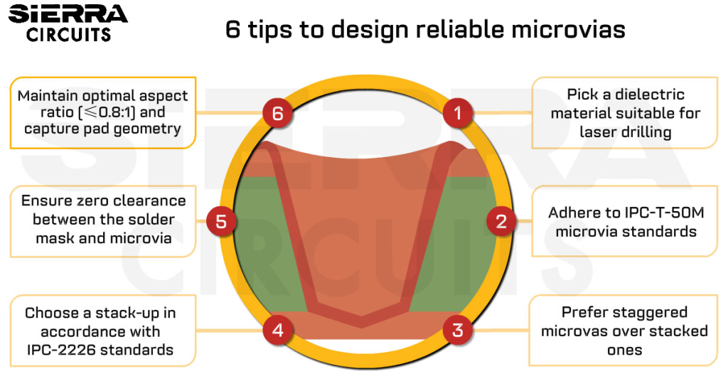
Key design strategies for enhancing microvia reliability include selecting suitable materials for laser drilling, adhering to IPC-T-50M guidelines, and implementing […]
HDI / Blind & Buried Vias
Via Filling Techniques Designers Need to Know for PCB Fabrication
PCB via filling is a technique in which the plated hole is filled with a conductive or non-conductive ... more »
PCB Manufacturing
How Via Impedance Impacts Signal Integrity in PCBs
Just like trace impedance, via impedance is also important in maintaining the signal integrity of your PCB design. ... more »
Signal Integrity
How to Design Reliable Microvias in Your PCBs
Key design strategies for enhancing microvia reliability include selecting suitable materials for laser drilling, adhering to IPC-T-50M guidelines, ... more »
HDI / Blind & Buried Vias
Via Filling Techniques Designers Need to Know for PCB Fabrication
PCB via filling is a technique in which the plated hole is filled with a conductive or non-conductive ... more »
PCB Manufacturing
How Via Impedance Impacts Signal Integrity in PCBs
Just like trace impedance, via impedance is also important in maintaining the signal integrity of your PCB design. ... more »
Signal Integrity
How Via Stitching Facilitates High-Current PCB Designs
Via stitching in high-current PCBs helps in creating proper ground connections, power distribution, and heat dissipation. These boards ... more »
PCB Design
Case Study: Designing 8 and 14-Layer HDI PCBs with Stacked Vias
Stacked vias are considered the most suitable solution for manufacturing HDI boards with advanced features. The configuration, with ... more »
Case Studies
Design and Manufacture of Staggered and Stacked Vias in PCBs
Staggered and stacked vias are well adapted nowadays. Their unique design enhances the density, as well as boosts ... more »
PCB Design
How to Design a Via with Current Carrying Capacity
The word ‘via’ is originally a Latin word that means road or way. In designing PCBs, vias play ... more »
PCB Design
PCB Via Design Using Altium Designer
The early days of PCB fabrication saw the exclusive use of through-hole vias that span the complete thickness ... more »
PCB Design
PCB Drilling Explained: The Dos and the Don’ts
Drilling is the most expensive and time-consuming process in PCB manufacturing. The PCB drilling process must be carefully ... more »
PCB Manufacturing


Fabrication, Procurement, & Assembly. PCBs fully assembled in as fast as 5 days.
- Bundled together in an entirely-online process
- Reviewed and tested by Engineers
- DFA & DFM Checks on every order
- Shipped from Silicon Valley in as fast as 5 days

Fabrication. Procurement & Assembly optional. Flexible and transparent for advanced creators.
- Rigid PCBs, built to IPC-6012 Class 2 Specs
- 2 mil (0.002″) trace / space
- DFM Checks on every order
- 24-hour turn-times available

Complex technology, with a dedicated CAM Engineer. Stack-up assistance included.
- Complex PCB requirements
- Mil-Spec & Class 3 with HDI Features
- Blind & Buried Vias
- Flex & Rigid-Flex boards