Contents

On-demand webinar
How Good is My Shield? An Introduction to Transfer Impedance and Shielding Effectiveness
by Karen Burnham
The early days of PCB fabrication saw the exclusive use of through-hole vias that span the complete thickness of the board. With the advent of surface mount technology, blind and buried vias were introduced, calling for complex via design practices. In this article, we will go over the fundamentals of via design using Altium Designer electronic design automation software.
Via overview
A via connects different layers in the PCB and is composed of a barrel, pad, and annular ring. A typical through-hole via will have pads on the top layer, bottom layer, inner layers, and the hole that goes through the pad. Therefore while designing the via, the pad sizes and hole sizes are defined. The different types of vias are as follows:
- Through-hole via – this via goes from the top layer to the bottom layer of the board.
- Blind via – this type of via goes from either the top layer or bottom layer to the layer immediately next to it, and does not travel through the whole board.
- Buried via – this via goes between two inner layers of the circuit board.
When the via is imported into the board it is assigned to a signal/net. This may be a power, ground, or signal name.
In the next sections, we will discuss the method in which the pad, hole sizes, and types of vias are defined and designed.
Via properties
PCB Editor object properties are options that are used to define the visual style, content, and behavior of the placed object. The property settings for every object type can be measured in two distinct ways:
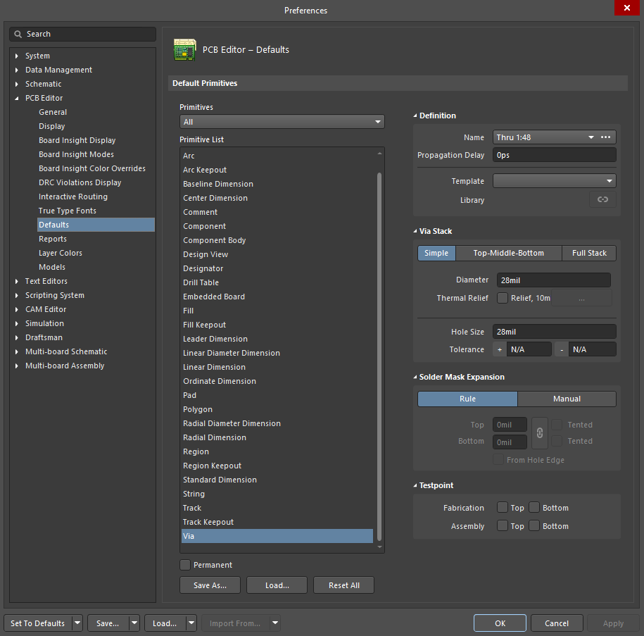
- Pre-placement settings – object properties for a via that can be logically defined beforehand are accessible as editable default settings on the PCB Editor. This is available on the defaults page of the preferences dialog that can be retrieved through the button at the workspace’s top-right part. The next step is to select the via object in the list of primitives to display the options on the right.
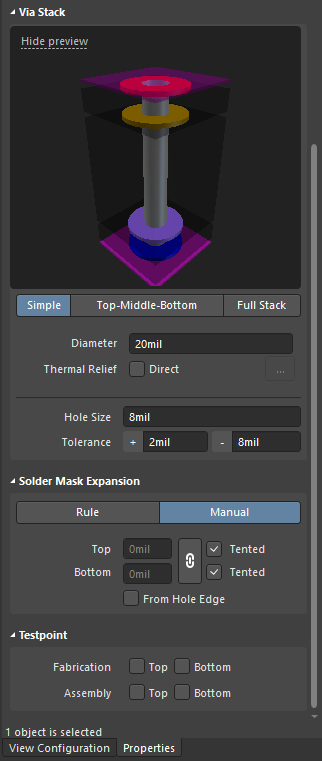
- Post-placement settings – each via object property can edited in the via dialog and properties panel when a placed via is chosen in the workspace.
Defining the via parameters
Here we get to define the via parameters as given below:
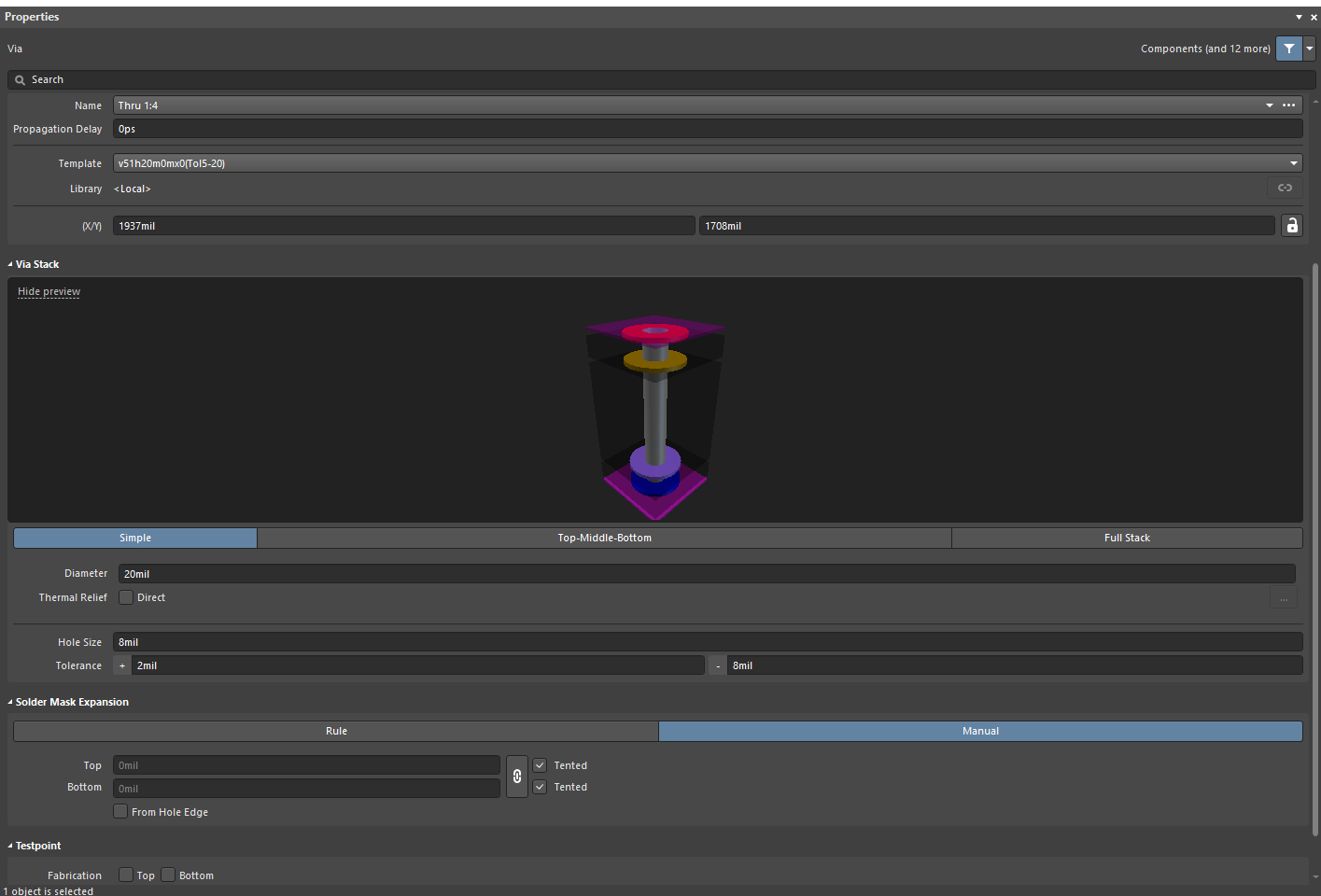
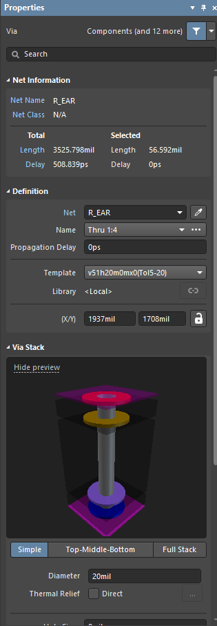
Net – utilize the drop-down list to choose the net that contains the via. Every net for the board design that is active will be displayed in the drop-down list. In case there is no net, click the assign net button to open the dialog for the net name. Here you can choose the required net in the design workspace by typing the net name.
Name – when one or more vias are selected, the via name is displayed by clicking the drop-down. This displays every via span that’s defined in the layer stack. All vias implemented on the board must be from the via spans defined in the layer stack.
Template – this displays the current template that is used for the via. To select another template, the drop-down menu can be used. In case there is a library associated with the template, it is displayed as well.
Library – this displays the via template that is stored in the current library. In case a via is placed from a pad library ( *.PvLib), it will include the library name in the specified field. After placement, the icon is enabled, indicating that the placed via properties are defined in the library and are not editable anymore. If the icon is not enabled, the contents can still be edited.
Propagational delay – this field displays the propagation delay, which is the period of time taken for the signal head to move from the sender to the receiver.
(X/Y) coordinates
X (first field) – this particular field displays the current X position of the via center to the current origin. You need to change the field value to alter the via position relative to the current origin. The field value can be added in imperial or metric units and can be changed according to the requirement. Units setting in the other region of the properties panel in the board mode can decide the default units when they have not been specified.
Y (second field) – This is for the Y position of the via center, and the same procedure can be followed as mentioned above.
Hole information
The fields that let you define the via hole parameters are as follows:
Hole Size – this field is meant to display the current hole size of the via. This parameter specifies the hole diameter in mm or mils to be drilled during manufacture. The hole shape can be circular, square, or slotted and the hole size can be set from 0 to 1000 mil. For mechanical holes (copper free) the hole size can be set to be larger than the via. You can edit the field value to change size according to requirements. The unit settings are identical to the one explained for the X Y fields.
Tolerance – The fits and limits of the board can be decided by setting the hole tolerance attributes. You can specify the minimum and maximum tolerances for the hole and there is no particular default hole tolerance value in Altium Designer.
Also read, How to Export Gerber and Design Files in Allegro
How do you set the size of a via in Altium Designer?
The size and shape of the via are defined as follows:
Simple – this option is used to choose a simple via.
- Diameter – enter the required diameter of the via in this field. The via diameter will be the same on every layer.
- Thermal Relief – select this box to introduce thermal relief required for mitigating heat conductivity. After checking the box, click the dialog for Polygon Connect Style in which you can select the connection style: Relief Connect, Direct Connect, or No Connect.

Top-Middle-Bottom – this option can be used to select varying diameters for the top layer, internal signal layers, and bottom layer.
- Displayed layer(s) – click a displayed layer to set the via dimensions for that particular layer. The layer that is selected will be highlighted.
- Diameter – click the drop-down and enter the required via diameter for the selected layer.
- Thermal relief – the process to set this variable is similar to the one in simple via.
Full Stack - this option is used to select a full stack via object.
- Displayed Layer(s) – the process to configure this is similar to the one used for “Top-Middle-Bottom”
- Diameter – click the drop-down and enter the required via diameter for the selected layer
- Thermal Relief – the process to set this variable is similar to the one in Top-Middle-Bottom vias.

The Z-plane or layer-spanning requirements of every via type can be defined using the via types tab. This tab does not define the size properties of the via, such as the diameter and hole size.
The size properties of the via are defined by:
- Editing a placed via manually in the properties panel
- Manually placing a via (Place>Via option) using the PCB default primitives
- Placing a via through interactive routing or autorouting using the routing via style design rule

Controlled Impedance Design Guide
6 Chapters - 56 Pages - 60 Minute ReadWhat's Inside:
- Understanding why controlled impedance is necessary
- Stack-up design guidelines
- How to design for impedance
- Common mistakes to avoid
Download Now
Defining a via type
To define the type of via you can refer to these steps:
- Defining a new via type will require one to switch to the via types tab in the layer stack manager. You can define the Z-plane layer-spanning requirements for every via type here, that will be needed for the design. When you open the tab for via types, it will include a single, thru-hole via type. A two-layer board will have the default via named as Thru 1:2. The convention here represents the via type and the first and last layers that the via spans. This default thru-hole span cannot be deleted.
- To edit the selected via type, you can use the layer stack manager mode within the properties panel. In case the panel is not visible, you can click the button at the right portion of the application to enable the same.
- To add via type, click the add button, followed by selecting the layers that the via type spans in the properties panel. The newly defined via type will have a naming convention as mentioned above, with the hole type and the first and last layer numbers. Based on the layers chosen, the software will automatically identify the via type ( buried, blind, and thru) and name the via type systematically.
- The span of the via type can be defined by configuring the first and last layer settings.
- In case of a µVia requirement, check the µVia box. This option is only present when the via spans adjacent layers or an adjacent layer +1 that is also known as a skip via.
- For the mirror option to be available, you need to enable the stack symmetry option in the board section of the properties panel. This mirror option is useful when you require a mirror of the current via that will span the symmetrical layers in the layer stack.
- Save the stack-up to update the changes in the PCB Editor.
Graphical editing
It is not possible to graphically modify the properties of a via other than the location.
- To move any via along with the linked tracks, click and hold, then move the via. The linked routing will remain connected to the via while moving it.
- To move any via without moving the linked tracks in the PCB library editor or PCB editor, choose Edit>Move, then click and hold to move said via.
Non-graphical editing
The following techniques of non-graphical editing are available:
Properties panel
Via properties can be edited using the properties panel in PCB Editor which enables editing of all items selected in the workspace. The Tab key can be used to access the panel during placement.
To access via properties of a placed via:
- Double-click on the via.
- Right-click on the via then choose properties from the context menu.
- If the Properties panel is already active, click once on the Via to choose it.
Editing multiple objects
In the properties panel, multiple objects can be edited using the property settings for any objects that are selected. Multiples of the same object type can be chosen manually through the list or filter panel or even the find similar objects dialog.
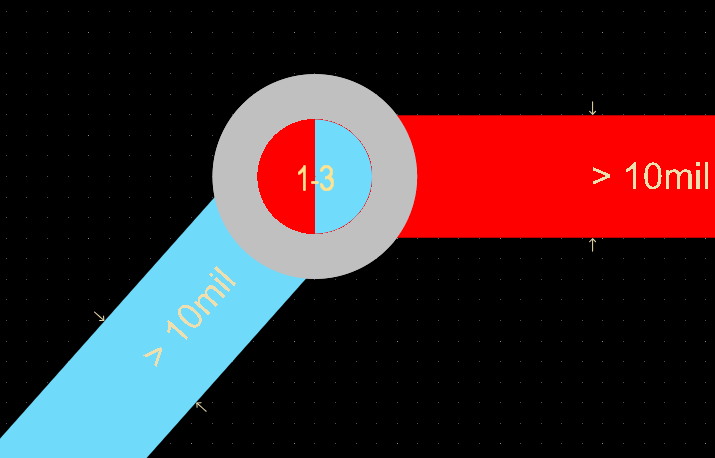
Via colors
Using the view configuration panel, you can configure the via colors. The via copper ring is shown in the multi-layer setting in the layers section. The via hole color is available in the via holes setting in the system colors section. One can also disable the hole display by toggling the desired settings.
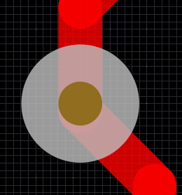
How do you select all vias in Altium Designer?
You can work with placed vias (vias that have already been defined) as follows:
The layer numbers in the span of the via can be shown within via types by toggling the via span display. This is available in the view options tab within the view configuration panel.

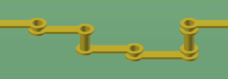
For stacked vias, the layer numbers displayed are the start and end layers of every via in the stack.
Working with stacked vias:
- While working with stacked vias, to form a continuous connection, click and drag the stack to move it as a whole, with the attached routing.
- To choose the uppermost via in the stack click once on the required via. To select the other vias in the same stack, use single clicks without moving the cursor.
- To move a single chosen via with the attached routing, use ctrl+click and drag it to the required location.
- To choose all vias in a particular stack, click once to select one, then press tab to apply the selection to all vias in the stack.
Net information
Net information is a group of parameters that are used to identify and specify a net and are as follows:
Net name – the name of the selected net.
Net class – the name of the selected net class.
Total length – the total signal length is the precise calculation of the total distance between nodes. Placed objects are evaluated to resolve overlapping or stacked objects, wandering paths within pads, and also the via length that is included. The pin package length is also included once it has been defined for pads. If the net has not been completely routed, the Manhattan length or (X+Y) length of the connection line is also included.
Total delay – the delay of the segments in the total length that have been routed. This includes the via and pad propagation delay values when they are defined for the vias and pads.
Selected length – the total length of the selected object(s).
Selected delay – the total delay of the selected object(s). This includes the via and pad propagation delay values when they are defined for the vias and pads.
How do you set via design rules in Altium Designer?
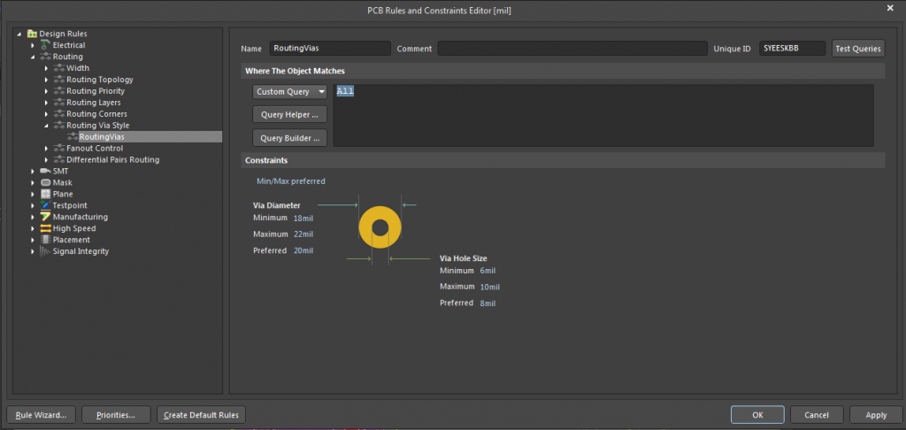
Here we will cover the routing via style design rule to define a via.
When you place vias during interactive routing, the size properties are defined by the applicable routing via style design rule. To place vias using the design rule, there is a set of via-related query keywords that can be used in the scope of rules.

| Via type query | Returns |
|---|---|
| IsVia | Every via object irrespective of the via type |
| IsThruVia | Every via that starts at the board top layer and extends to the bottom layer |
| IsBlindVia | Every via that starts on a surface layer (top/bottom) and ends on an internal layer, except for µVias |
| IsBuriedVia | Every via that begins on an internal layer and ends on another internal layer, except for µVias |
| IsMicroVia | Every via that has the µVia option enabled and connects adjacent layers |
| IsSkipVia | Every via that has the µVia option enabled and spans 2 layers |
When you implement a layer change while routing, the software will check for the start and stop layers in the layer change. This is while selecting a via type from the layer stack manager. Next, it detects the highest priority applicable to the routing via style design rule and implements the via size settings. The settings are applied through the constraints section of the rule for the via being placed.
As discussed, you need to select the via type from a broad selection of vias for your PCB design to optimize board specifications. Reliable and high-performance multi-layered boards call for efficient via design implemented by expert designers in the manufacturing facility.
If you want to learn more about via design, drop us a comment below. Read our post on how to design a via with current-carrying capacity to understand the basics of via current capacity, multilevel optimized interconnection, etc.
High-Speed PCB Design Guide
8 Chapters - 115 Pages - 150 Minute ReadWhat's Inside:
- Explanations of signal integrity issues
- Understanding transmission lines and controlled impedance
- Selection process of high-speed PCB materials
- High-speed layout guidelines
Download Now


