Contents

On-demand webinar
How Good is My Shield? An Introduction to Transfer Impedance and Shielding Effectiveness
by Karen Burnham
Our PCB design engineers worked on a medical circuit board for a healthcare device: an advanced optical scanner for ophthalmology.
The primary objective of this project was to integrate an optical scanner with a PCB to control the scanner’s movement in the X, Y, and Z directions. This integration enables the capture of detailed eye images.
The board layout comprises critical components such as stepper motor connectors, inductors, switching regulators, motion controllers, and microcontrollers.
In this case study, you’ll learn how we resolved EMI and routing issues in a medical PCB.
Highlights:
- To reduce EMI radiation in the inductor circuit, we isolated it from sensitive components and placed shielding vias around it.
- To route high-current traces between the stepper motor connector and the driver, we adopted polygons to ensure ample current flow.
- To break out the LQFP microcontroller, we utilized layers 3 and 6 and routed signals beneath the package.
Optical scanner PCB design specs and stack-up configuration
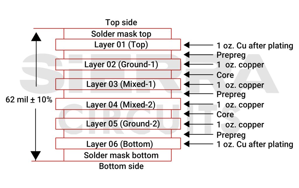
- Number of layers: 6
- Board thickness: 62 ± 10% mil
- Board dimension: 127 mm x 88.9 mm
- Build class: IPC-6012 class 3
- Finish copper thickness: 1 oz. on all layers
- Dielectric material: Ventec VT-47
- Surface finish: ENIG
- Electronic and electromechanical components: Stepper motor connector and driver, encoder connector, motion controller, microcontroller, limit switches connector, joystick connector, USB connector, power input connector, LDO, and DC-DC booster
- Signals: 90 Ω differential pair controlled impedance traces, with a width of 6.5 mil and spacing of 5 mil
- Maximum working signal frequency: 72 MHz
- Working voltage rating: 24 V
- Maximum current rating: 6.5 A
- Plated hole: Size ranges from 8 to 120 mil
- Non-plated hole: Size ranges from 36 to 118 mil
- The circuit board build-up is symmetrical, comprising ground and mixed-signal layers.
EMI and routing issues faced in this optical scanner PCB
Challenge #1: Addressing EM radiation
Managing EM radiation posed a significant obstacle in the inductor and switching regulator circuit. This section had the potential to induce noise interference in the digital circuit.
Solution: Isolate the inductor section from sensitive components
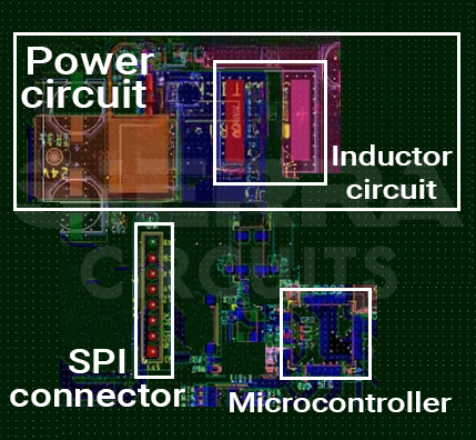
The primary focus was to isolate the inductor section from sensitive components like crystal and microcontroller to prevent noise generation. This required careful placement and positioning of components.
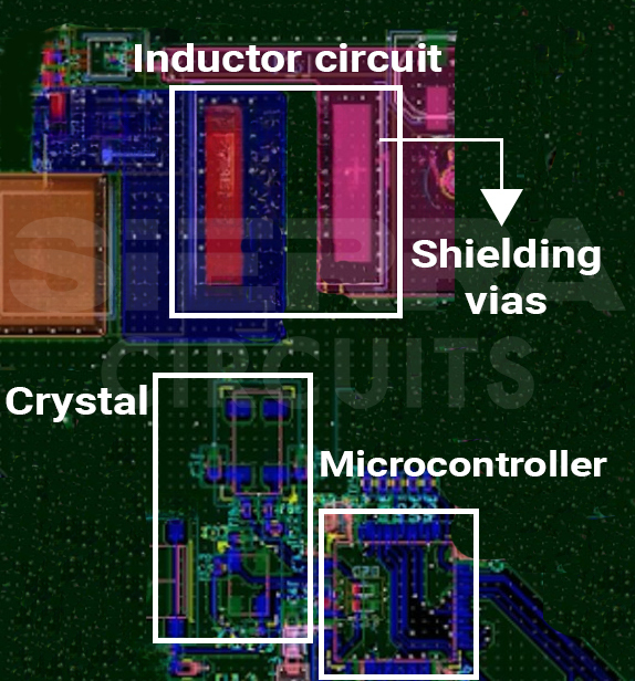
We adopted a thorough iterative process to identify the optimal position for the crystal and microcontroller. The placement, as shown in the image above, ensures effective isolation from the inductor and switching regulator to minimize the risk of EMI.
Furthermore, we placed shielding vias around the inductor circuit to create a barrier against electromagnetic emissions. For more, read tips and PCB design guidelines for EMI and EMC.
To learn about class 3 PCBs for medtech, download our IPC Class 3 Design Guide.
IPC Class 3 Design Guide
8 Chapters - 23 Pages - 35 Minute ReadWhat's Inside:
- IPC guidelines for manufacturing defects
- IPC standards for assembly processes
- Common differences between the classes
- IPC documents to set the level of acceptance criteria
Download Now
Challenge #2: Routing high-current paths through stepper motor
Routing high-current traces between the stepper motor connector and the driver increases the risk of overheating due to the confined space for the current flow.
Solution: Implement polygons to route high-current paths
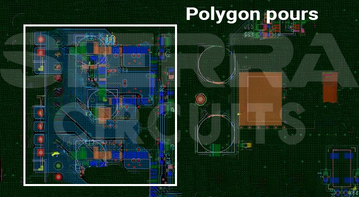
To overcome this routing issue, our PCB layout engineers opted for polygons instead of traces.
Unlike traces, polygons offer a more expansive area for current flow, eliminating the limitations associated with traditional routing methods.
By utilizing polygon pours, we established a seamless connection between the stepper motor connector and the driver. This provided ample room for high currents to flow without the risk of overheating.
When it comes to medical devices, precision and reliability are paramount. Sierra Circuits fabricates and assembles cutting-edge healthcare and medical-grade PCBs that meet stringent industry standards such as ISO 13485:2016
Challenge #3: Breaking out the microcontroller
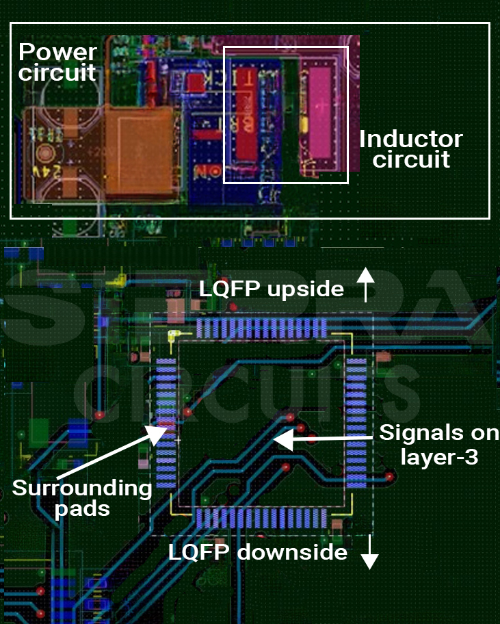
Routing the LQFP microcontroller with 64 pins posed a significant challenge due to the presence of surrounding pads and an inductor circuit. This complexity made it difficult to route signals in different directions with optimum spacing.
Solution: Utilize the inner and bottom layers to route microcontroller signals
Microcontrollers are typically placed at the center, and all the components connected to them are placed around them to ease the routing process. However, the presence of the power section on the upside of the LQFP required a deviation from conventional placement strategies.
To address the above challenge, components were shifted to the microcontroller’s downside. All the connections were routed carefully, considering the spacing requirement of the connection and surrounding pads. We utilized layers 3 and 6 to break out the LQFP.
Additionally, the circuit design involved routing a common SPI (serial peripheral interface) line to connect five ICs via one main connector. We adopted a daisy chain routing approach where the common SPI line was sequentially connected from one IC to the next, forming a chain-like configuration. Explore the role of UL standards in ensuring medical circuit board performance and safety in critical applications.
This routing approach streamlined the signal transmission along the common SPI line. This facilitates communication between the connected ICs and contributes to the overall functionality.
We have summarized the challenges and the solutions to overcome them in the table below:
| Challenges | Solutions |
|---|---|
| EM radiation | Isolate the inductor section from sensitive components such as microcontroller and crystal Place shielding vias around the inductor circuit |
| Routing high-current path | Employ polygons pours instead of traces |
| Breaking out the microcontroller | Strategically place components around the microcontroller and utilize inner and bottom layers to route signals from the microcontroller |
For more medical board design tips, see medtech PCB design considerations with IPC and UL standards.
Key takeaways
- Strategic component placement and shielding techniques are essential to effectively manage EMI radiation and high-current routing challenges.
- Adopting polygon-based routing and daisy chain configurations enhances signal transmission efficiency and overall functionality.
- Complex package configurations, such as LQFP with surrounding pads, require careful routing techniques and innovative placement strategies to ensure optimal functionality.
Check out our PCB design services for customized solutions that match your unique circuit board requirements.
Through the collaborative efforts of our layout designers and product stakeholders, we engineered an advanced 6-layer board, significantly enhancing optical scanner capabilities for ophthalmology applications.
Need assistance designing your healthcare circuit board? Post your questions on our PCB forum, SierraConnect, and our experts will answer them.
Check out our series of design case studies, covering topics such as integrating antennas with microcontrollers and handling the complexities of HDI boards with BGAs.
About Mohamed Faheemuddin : Mohamed Faheemuddin is a mechanical engineer. His passion for electronics drew him to the PCB industry. With an experience of over 3 years in the PCB industry, he specializes in developing articles for engineers and hardware designers.









I see that you have used polygons to route high-current paths. Are there are any other techniques to route them without the risk of overheating?
I’m laying out a BGA for the first time and feeling a bit overwhelmed with some of the finer details. It’s a 9x9 BGA with a 0.4mm pitch, so I’ve opted to use vias in pads (filled) to break out the signals.
My question pertains to the bottom layer of the board beneath the BGA. It’s currently empty, and I’m considering placing passive components directly below the BGA and using filled through-holes to connect them to the bottom layer of the board. Is this a viable approach, or are there potential issues I should be aware of?
While many resources online focus on fan-out strategies for BGAs resembling QFP MCUs, I’m unsure if this is necessary for my particular BGA. Any insights or advice would be greatly appreciated.
Although a 0.4 is a fairly tight pitch, you’re luck you only have potentially 81 pins to deal with. Going with via-in-pad will also make the job much easier. And, if you’re referring to the bypass caps as the “passive components” then you should be right on target. Assuming you don’t violate any clearances or placement rules, placing those caps directly underneath and keeping them as close to the pin (ball) as you can, you should get about as good of results as is possible. For a small BGA like this the fanout should be both fairly obvious and fairly easy. If you find yourself facing larger BGA packages in your upcoming projects you might want to take a look at BGA Breakouts and Routing by Charles Pfeil, published by Mentor Graphics. It shows lots of examples and provides some insight as how to go about finding the best approach.
Yes. You can use a plane to handle high current requirements.