Stacked and Staggered Vias to Optimize PCB Design and Manufacturing

Amit Bahl
CRO
Sierra Circuits
Fill out the form:
Understanding stacked and staggered vias
HDI technology ensures comprehensive control over signal integrity and offers superior electrical performance compared to standard PCBs. Stacked and staggered vias are the driving factors in high-density boards since they enable dense component placement and versatile routing with optimized cost.
Staggered microvias have separate drill axes and are positioned offset to each other. For a perfect staggered design, the vertical separation between the centers of two microvias should be greater than the microvia diameter. So, if your board demands tight spacing restrictions, staggered vias might not be the best choice. These vias can withstand multiple thermal cycles and reduce signal reflection by trimming down the stub lengths.
Unlike staggered, stacked vias share the same drill axis. They maintain a consistent trace geometry, providing uniform impedance. The primary concern here is the reliability. When pressure is exerted on these microvias from the z-axis of the dielectric, it can lead to barrel and corner cracking. This occurs due to a mismatch in the CTE of the materials. The risks increase as the layer count goes beyond two.
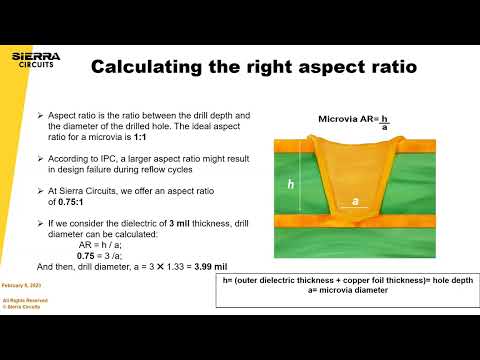
The other key factor in designing microvias is the aspect ratio. IPC recommends an aspect ratio of 1:1 for the holes whose depth is less than 10 mils. Lower aspect ratio guarantees even plating and provides great mechanical strength. This determines the reliability of your board. Similarly, there are many more things to consider while designing an HDI PCB.
In this webinar, our PCB design and manufacturing experts will take you through the specifics concerning staggered and stacked vias. This will help you in choosing the right HDI structure for your design.
What you’ll learn:
- Design and manufacturing rules for staggered and stacked vias
- Constraints that you need know before implementing staggered and stacked microvias
- Why aspect ratio is a critical parameter for microvia reliability?
- Need for sequential lamination and copper filling
- How stacked and staggered vias affect the board cost
- Best stack-up designs involving staggered and stacked vias
Presented by Amit Bahl
Amit has been in the PCB industry for 20+ years. He is the Chief Revenue Officer at Sierra Circuits. His passion is to empower tech companies to achieve their visions and change the world. Rockets going into space, self-driving cars taking up the streets, cancer-fighting medical devices, protecting the country, he’s ready to build any circuit board!
Watch the Trailer