


Contents

On-demand webinar
How Good is My Shield? An Introduction to Transfer Impedance and Shielding Effectiveness
by Karen Burnham
Replication of design blocks is essential to reduce the complexity of your board layout. This is accomplished in your EDA tools by applying a feature called auto grouping of repetitive PCB design blocks.
Modern circuit board design tools offer various techniques to group elements together and reuse them in your PCB layout. This feature will enable you to automatically route and lay out circuits that are similar.
In this article, you will learn the grouping of repetitive blocks using Altium Designer and Allegro.
What are repetitive design blocks?
A circuit board schematic can have several component blocks that need to be used repeatedly. Creating these recurring circuits can be time-consuming. To overcome this challenge, you can create a component room and define it for replication. These rooms are called repetitive design blocks.
In the following sections, we will demonstrate the steps involved in auto grouping circuit elements in Altium Designer and Allegro design tools.
Auto grouping design blocks in Altium Designer
Once you define a room with a set of components, you can implement the configuration in your layout repetitively with ease. In Altium Designer, you can also store certain sections of your design as snippets (only for reference) or circuit blocks after creating a room.
What is a room object in Altium Designer?
In addition to the reuse features, Altium Designer has a unique room object to auto-group repetitive components. These rooms can be orthogonal, non-orthogonal, and rectangular-shaped.
Some of the unique characteristics of this feature are:
- It allows you to create Altium rooms in the schematic to relocate a large set of components, duplicate numerous circuit blocks, and apply design rules to a group of components.
- The creation of rooms before placing the components speeds up data transfer from the room objects to the schematic.
- It enables you to define a component class for each component in the room. With this, you can establish precise design guidelines for individual elements.

High-Speed PCB Design Guide
8 Chapters - 115 Pages - 150 Minute ReadWhat's Inside:
- Explanations of signal integrity issues
- Understanding transmission lines and controlled impedance
- Selection process of high-speed PCB materials
- High-speed layout guidelines
Download Now
Creating Altium rooms for auto grouping
Add the repetitive components and create a room object. You can replicate the circuits by following the below steps.
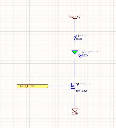
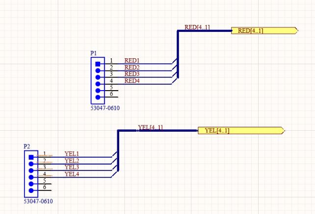
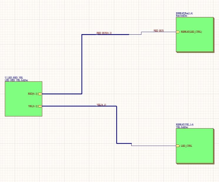
1. Create the schematic by using the “repeat function”
You can access the repeat function using the shortcut Shift+Cntrl+R. Now, choose the blocks which need to be replicated. The screenshots below depict the schematic, connectors, and signal path created using the repeat function.
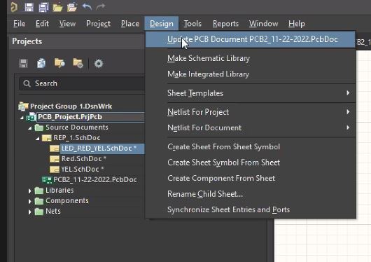
2. Import the netlist into the layout
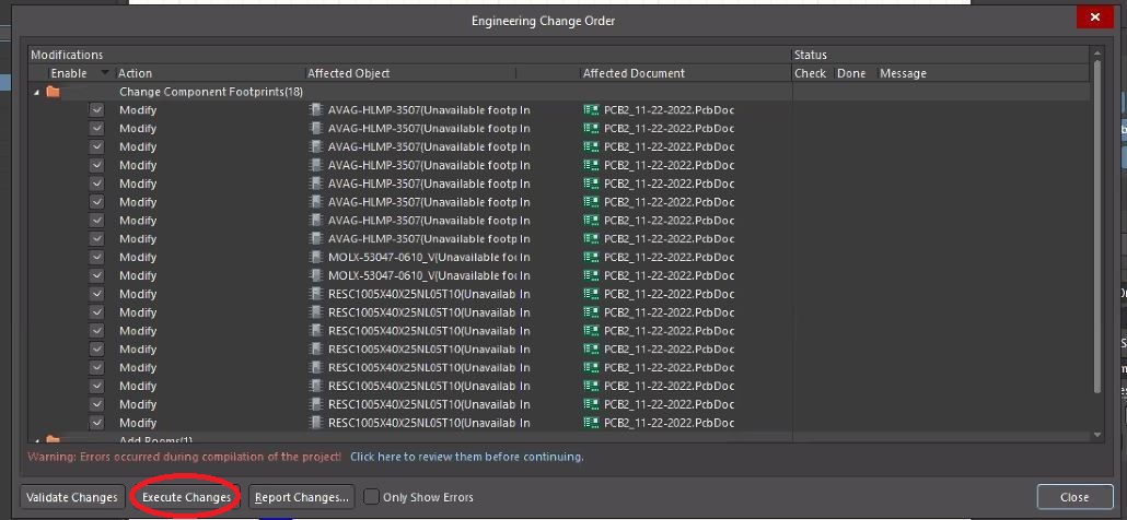
Once the schematic is created, you need to import the netlist in the layout. Go to Update PCB Document PCB1 under the Design tab and click on execute changes after selecting the required netlist. This will automatically update the connections of the components which are designated in the room.
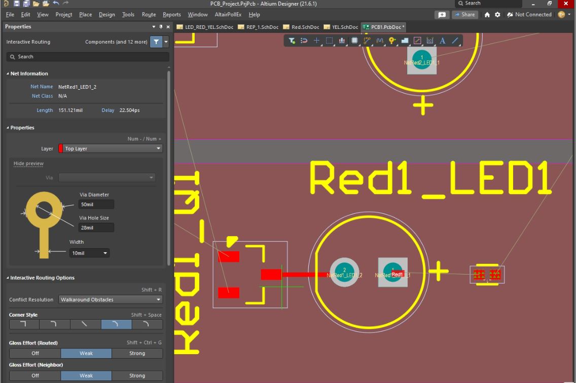
3. Route the components in one room
After importing the netlist, you can make the necessary routing, via placement, and silkscreen adjustments in a room.

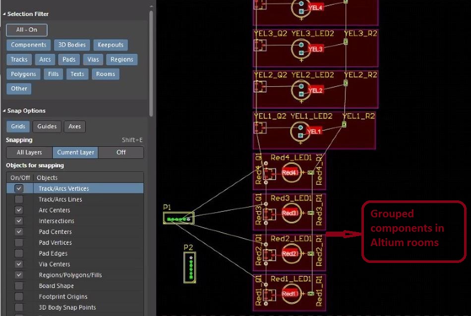
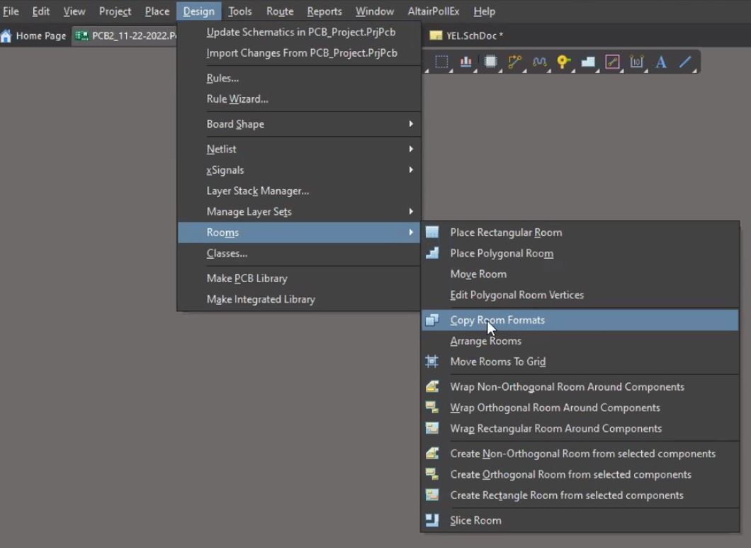
4. Use the copy room format option to incorporate the changes in all the rooms
To apply the changes in all the rooms, you need to choose the option Copy Room Formats and click on the other rooms that need to be duplicated.
The rooms will be duplicated as shown in the below screenshot after executing the copy room format function.

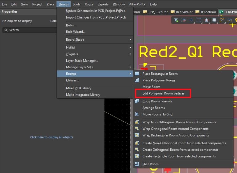
If you’d like to edit the shape of the rooms, go to the option Edit Polygonal Room Vertices under Rooms in the Design tab.

PCB Design for Assembly Handbook
6 Chapters - 50 Pages - 70 Minute ReadWhat's Inside:
- Recommended layout for components
- Common PCB assembly defects
- Factors that impact the cost of the PCB assembly, including:
- Component packages
- Board assembly volumes
Download Now
Auto grouping in Allegro
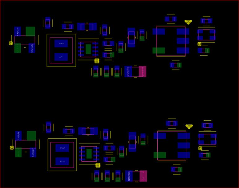
Auto grouping in Allegro simply means organizing randomly placed components. Your design may contain a group of two or more identical blocks as shown in the schematic below. Reusing these designated blocks will be more convenient.
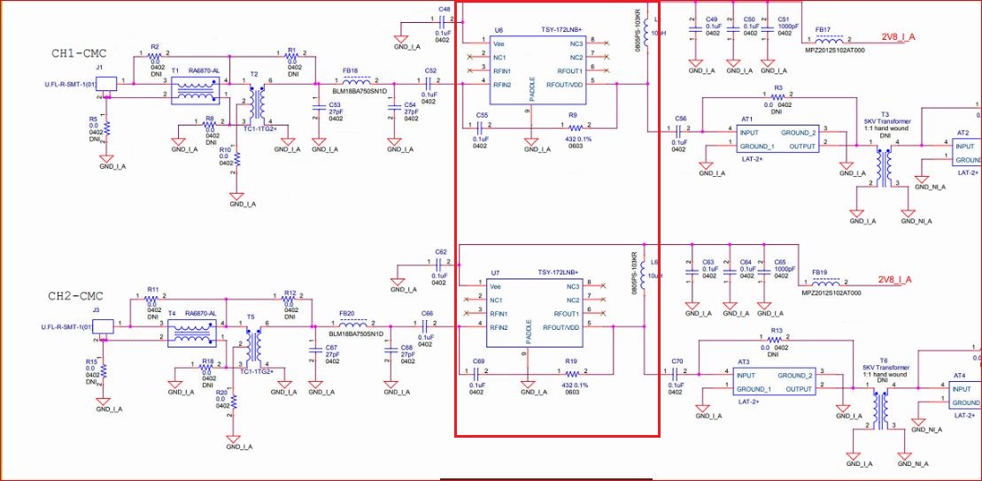
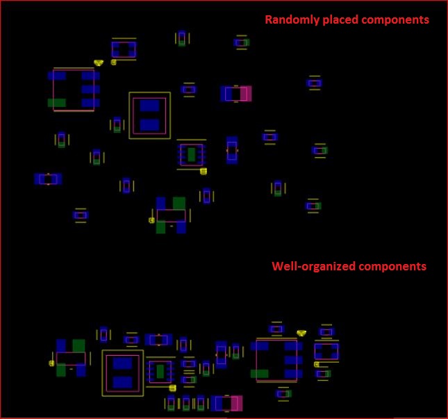
As you can see, the above schematic has three different sections with the same circuitry. This means that the component placement is identical in all the circuit blocks. In the image below, there are two sets of components. One among them is well organized and the other is randomly placed.
Now, we’ll have a look at the steps to automatically organize the randomly placed components in your layout.
- Creation of module definition file
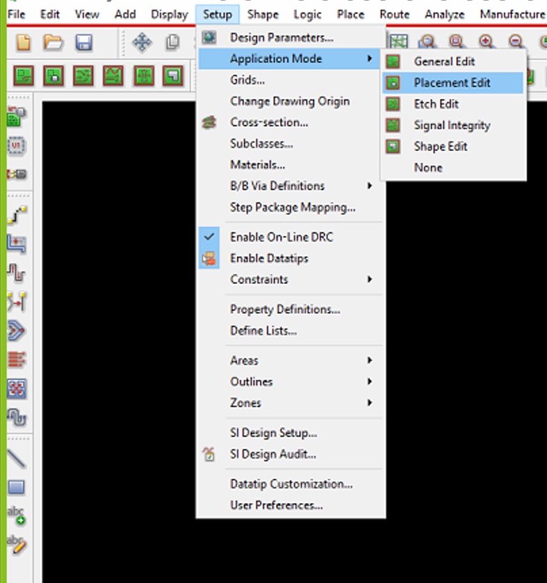
Select the option Placement Edit under Application Mode in the Setup tab.
Now, select the components that are well-organized.
After selecting the components, right-click, choose the option Place replicate create and hit continue.
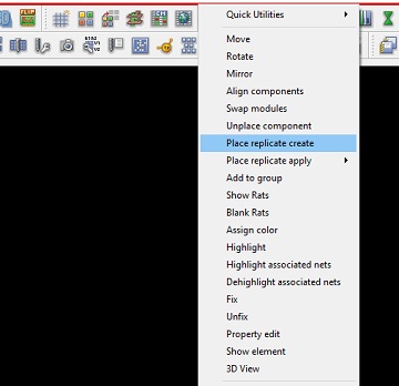
Next, hover your cursor over the well-organized component region, right-click, and hit done. Now, left-click on the same region. This pops up a window asking you to save the module definition file. Ensure that you save this file in the same location where your design files are present.
Read how modular PCB design method simplifies complex layouts to know more.
2. Use the module definition file to organize the randomly placed components
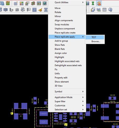
First, select all the components that you need to organize.
Now, right-click, choose the option Place replicate apply, and select the module definition file you just created.
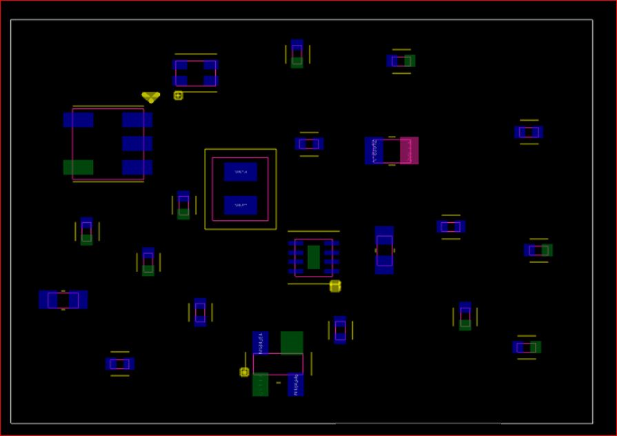
The components will now be auto-grouped as shown below.
Need help in designing reliable PCBs? Our engineering team can help you with thermal management, stack-up design, and DFM analysis.
You can book a meeting with our experts or call us at +1 (800) 763-7503.

How to prevent mistakes in auto-grouping repetitive PCB design
- Avoid using circuits from old designs. Sometimes this old circuitry which consists of old components (obsolete components) will not be available during the board manufacturing process. This will force you to redesign the entire layout.
- Follow the schematic to place the grouped components on the board. This will increase signal integrity.
- Use an updated library.
- Cross-verify the components and the available datasheet. There are possibilities for variation in component footprints and technical datasheets.
- Focus on design synchronization. Ensure that the schematic and the layout are in sync, after grouping the repetitive blocks.
- Complete the stack-up before laying out the board, else you may have to redo the layout or move the layers to rectify associated problems.
- Provide sufficient space for routing after grouping the design blocks to achieve desired controlled impedance.
- Make sure that the replicated block and the location where you use this block have the same number of components.
To know how to design a castellated board, see how to design a castellated circuit board using Altium Designer and Allegro.
Avoiding repeated blocks in your design is inevitable. It makes perfect sense to include these blocks as a cluster in the layout. Grouping promotes efficient thermal management, reduces EMI, and aids in optimal routing. Let us know, below in the comment section, if you have any queries related to the grouping of repetitive design blocks.


