


Contents

On-demand webinar
How Good is My Shield? An Introduction to Transfer Impedance and Shielding Effectiveness
by Karen Burnham
When it comes to designing HDI PCBs, a plethora of challenges await, including complex routing requirements, issues related to propagation delays, electromagnetic effects, and impedance mismatches. To fully harness the potential of high-density boards, consider signal integrity to avoid issues like crosstalk and signal reflection.
Highlights:
To maintain signal integrity in HDI boards:
- Select a dielectric material with low Dk (<4) and Df (≃ 0.001)
- Place the signal layers between the ground planes
- Place microvias as close as possible to the signal pads to avoid impedance discontinuities
- Place the decoupling capacitor close to the power pins to ensure power integrity
6 common challenges in designing a high-density board
High-density circuit boards call for fine traces, low-impedance power distribution, varied trace lengths, uniform impedance, and effective thermal dissipation. As a PCB designer, you should know these challenges and implement the right techniques to overcome them.
Knowing the potential hurdles enables you to craft your design in alignment with standard HDI PCB specifications.
Here are the six common high-density design challenges:
- The increased component density and multiple signal layers result in complex routing requirements within a limited space. This leads to routing congestion and increases the risk of crosstalk.
- Traces of varying lengths due to a compact layout can lead to propagation delays and skew between signals.
- Impedance mismatch in HDI due to insufficient trace widths and spacing causes signal reflections and signal degradation.
- The compact layout can make it challenging to ensure low-impedance power distribution and effective decoupling, leading to voltage fluctuations.
- For HDI designs operating at high frequencies, electromagnetic phenomena such as skin effects and dielectric losses become significant, leading to signal attenuation and distortion.
- Miniaturized components, densely packed traces, high-speed signal switching, and component power dissipation can lead to localized heating, damaging ICs.
To learn the ways to mitigate routing challenges in high-density boards, read 5 HDI PCB routing challenges with solutions.
10 best design practices for HDI PCB signal integrity

The primary goal here is to equip you with practical tips and techniques to maintain optimal signal integrity in your high-density PCB layouts. From stack-up design to controlled impedance, we will explore various design strategies that can help you create a reliable high-density circuit board.
1. Choose a material with low Dk and Df
The success of high-density designs heavily relies on the careful selection of appropriate HDI PCB materials that can considerably impact signal integrity, thermal management, and overall performance of your design.
Consider these factors when you select dielectric materials:
- Choose a material with a low dielectric constant (<4) for lesser signal distortion and propagation delays.
- A lower dissipation factor (≃ 0.001) indicates lower energy loss in the substrate, ensuring reduced signal attenuation and quality preservation.
- Higher thermal conductivity materials offer effective heat dissipation, preventing thermal hotspots and ensuring stable signal performance.
Tip: When you pick materials for HDI, you need to consider the operating frequency of your design.
Here are a few typical HDI materials:
- Normal speed and loss: N7000-2HT, and Isola FR370HR
- Medium speed and medium loss: FR408HR and Isola I-Speed
- High speed and low loss: I-Tera MT40 and Megtron6 R-5775
- Very high speed and very low loss (RF/microwave): Isola Tachyon 100G, and Astra MT77
For complete guidance on designing an HDI circuit board, download our e-book.

HDI PCB Design Guide
5 Chapters - 52 Pages - 60 Minute ReadWhat's Inside:
- Planning your stack-up and microvia structure
- Choosing the right materials
- Signal integrity and controlled impedance in HDI
- Manufacturing considerations for higher yields
Download Now
2. Place signal layers between ground planes for a low-impedance return path
The arrangement of different layers of materials that make up the PCB plays a crucial role in maintaining signal integrity. Choosing suitable layers to design the HDI PCB stack-up configuration can significantly influence signal integrity and minimize noise.
During the layout design, you must precisely choose the number of signal layers, ground plane arrangement, and power plane distribution to minimize signal distortions.
- Place high-speed signal layers between ground planes to shield against EMI and provide a low-impedance path for return currents.
- Use adjacent signal layers with orthogonal routing to minimize electromagnetic coupling.
- Assign specific layers within your stack-up for critical controlled impedance traces.
- Include dedicated power planes to provide a stable power distribution network and reduce voltage drop.

- Maintain symmetry in the stack-up whenever possible to achieve consistent impedance.

3. Implement efficient trace routing to mitigate impedance mismatch
Controlled impedance routing in high-density boards ensures signals travel with minimal reflections and degradation. This can be achieved when trace routing is efficient and accurate. Impedance can be controlled using specialized trace geometries, such as microstrip and stripline.
Stick to these guidelines to avoid impedance mismatch in your design:
- Choose dielectric materials with a stable dielectric constant as they affect the propagation speed of signals and, consequently, their impedance.
- Determine which layers of your HDI PCB will require controlled impedance traces.
- Implement a proper termination technique, such as parallel, series, or Thevenin termination methods, to avoid signal reflections for optimal signal integrity.
- Use differential pair routing for signal integrity enhancement, where two complementary signals are transmitted simultaneously to reduce noise and enhance signal quality, which requires careful length matching.

- Maintain a solid and continuous return path for each signal trace, preferably on a ground plane adjacent to the signal layer, to ensure a low-impedance path.
4. Have microvias close to the signal pads to avoid signal reflections
Microvias play a significant role in reducing via stubs, contributing to enhanced signal integrity. The primary purpose of designing microvias is to route high-speed signals through shortened paths, which can reduce reflections and attenuation.
Keep these things in mind when you’re designing microvias:
- Place microvias as close as possible to the signal pads they connect to. This minimizes trace length, reduces impedance discontinuities, and maintains high-speed signal integrity.
- Consider using microvias in pad (VIP) technology to route signals directly from the BGA pads to inner layers, reducing via count and trace length.
- Keep the microvais away from sensitive circuitry, such as analog components, sensitive sensors, or low-level analog signals, as they can introduce noise or interference.
- Minimize the number of vias through the transmission line as much as possible. Longer signal paths with multiple vias can introduce signal degradation and increased impedance.
- When routing differential pairs, ensure that the microvias for each pair are placed symmetrically and have equal lengths to maintain balance.
- Avoid clustering microvias together in a small area, as this can lead to uneven impedance and crosstalk between nearby traces.
PCB expert design tip:
Daniel Beeker, Technical Director at NXP Semiconductors, explained, ” Ground transition vias are the key to good signal integrity and EMI control. I always place them as close to the signal vias as allowed. For the field to be contained, you need two distinct conductors separated by a space. For good power delivery in the Z axis, interleaved power and ground vias are required. Interleaved vias form multiple parallel Z-axis transmission lines connecting the horizontal dielectric layers in what I call a waterfall.”
He further added, “For my ground flood areas, I add a ground via wherever they cross on other layers, to help form a pseudo-Faraday cage in my PCB structure. For the boundary edges of ground flood structures, sometimes I do have perimeter stitching vias, but only if the signals that are adjacent to these flood areas are switching faster than 200 ps.”
5. Position decoupling capacitors close to the power pins for power integrity
Designing a stable power distribution network (PDN) is instrumental for signal integrity in HDI PCBs. Creating a proper power plane can help minimize voltage fluctuations and reduce noise, and managing PDN impedance ensures stable power for high-speed signals. See what Steve Sandler has to say about power integrity in PDN design and high-speed simulations.
Another issue that you need to address is power integrity, which is handled by placing decoupling capacitors near active components. These decoupling capacitors are essential in providing clean power to components and mitigating power-related signal noise and disturbances.
- Place decoupling capacitors as close to the power pins of the target components as possible.
- Minimize the loop area between the component, the capacitor, and the ground connection to maximize noise reduction.
- Maintain a minimum clearance of 50 mil between power traces and the board edge.

- Connect one terminal of the decoupling capacitor to the power plane and the other terminal to the ground plane to ensure that the capacitor effectively shunts noise to the ground.
- Choose decoupling capacitors with appropriate capacitance values and voltage ratings based on the frequency of the noise and the power demands of the component.
- Create a dedicated trace for each decoupling capacitor that connects it directly to the ground plane or a solid ground reference. All capacitors should be connected to the ground plane in parallel. The trace should be as short and direct as possible to minimize inductance.
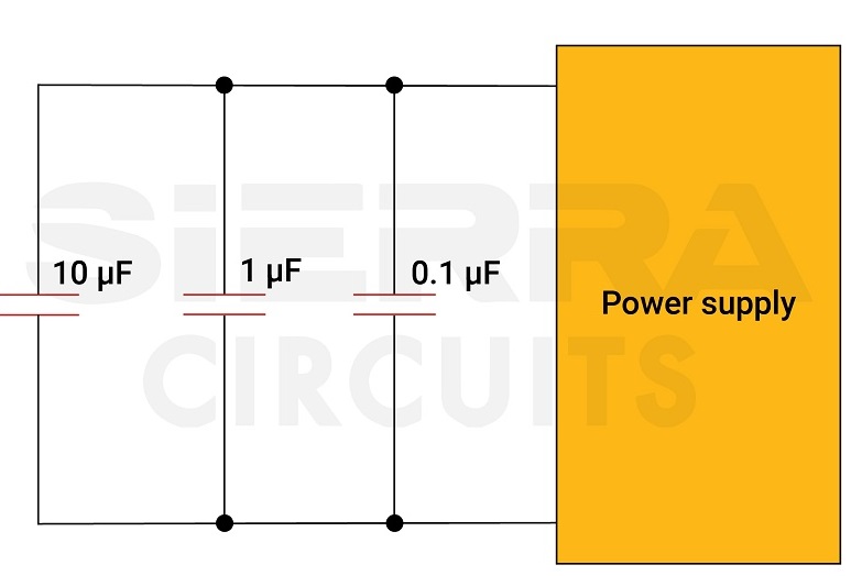
- Place the lowest-valued capacitor closest to the IC’s pin to minimize trace loop area. Consecutively, place higher-valued capacitors progressively farther away from the IC pin.
See 4 common PDN design challenges and how to resolve them to mitigate PDN noise in circuit boards.
6. Utilize guard traces between high-speed traces for crosstalk reduction
Signal crosstalk occurs when one signal interferes with another; in other words, it is an unwanted coupling of signals between adjacent traces, leading to signal degradation in high-density PCBs. In high-speed HDI PCBs, it is essential to avoid signal crosstalk to maintain data integrity.

To reduce crosstalk:
- Increase the spacing between high-speed signal traces, as wider spacing helps lower the coupling effect, diminishing the likelihood of crosstalk.
- Implement guard traces or guard vias between sensitive high-speed signal traces that act as barriers, shielding signals from adjacent traces and reducing crosstalk.

- Ensure a solid ground plane beneath and in between high-speed signal layers to provide a reference plane for signal return paths and to minimize crosstalk.
- Make use of differential signaling for high-speed data lines as they have inherent noise-cancellation properties, reducing the impact of crosstalk.
For more on crosstalk reduction techniques in HDI, read how to avoid crosstalk in HDI substrate.
7. Incorporate shielding and grounding techniques to reduce EMI
High-speed signals in HDI PCBs can generate EMI and EMC issues. This can adversely affect signal integrity and can potentially cause device malfunctions. To avoid this:
- Create a solid ground plane to serve as a reference for signal return paths.
- Do not split the ground plane to minimize electromagnetic radiation.
- Use differential signaling for high-speed signals to improve noise immunity and reduce crosstalk.
- Use shielding techniques like metal shields, Faraday cages, and via stitching across board edges and connecting ground planes with low impedance to contain electromagnetic radiation.

- Use via stitching techniques to connect ground planes across different layers. This helps provide a low-impedance return path for signals and reduces ground bounce.

- Incorporate signal transition vias whenever there is a change in the reference plane.
Further, adherence to applicable EMI/EMC standards guarantees that HDI PCBs meet regulatory requirements and perform reliably in their intended applications. For design considerations and fabrication challenges of UHDI boards, see designing and fabricating ultra-HDI PCBs.
Download our design guide to learn how to design boards with signal integrity.

Signal Integrity eBook
6 Chapters - 53 Pages - 60 Minute ReadWhat's Inside:
- Impedance discontinuities
- Crosstalk
- Reflections, ringing, overshoot and undershoot
- Via stubs
Download Now
8. Implement thermal vias for effective heat dissipation
The need for thermal management in HDI PCB is crucial. Excessive heat can cause a reduction in timing margins that causes electronic components to operate more slowly. This can potentially lead to problems in meeting specified timing requirements, causing errors in data reception.
Additionally, some electronic components may exhibit increased conductivity at higher temperatures, leading to faster signal propagation and, therefore, circuits running faster. If a signal arrives at its destination before it is expected, it can overlap with the next clock cycle or data transition, leading to data corruption.
Elevated temperatures in a PCB can lead to an increase in the current drawn by the components, causing them to consume more power. This excess current through PCB traces gives rise to electromagnetic interference (EMI), which can couple with nearby signals, resulting in communication errors and signal distortion.
Consider these thermal design strategies to avoid data corruption:
- Select an appropriate PCB material that offers high thermal conductivity to preserve signal integrity. Isola Tachyon 100G, Astra MT77, and I-Tera MT40 are a few among the high thermal conductivity materials.
- Identify and address thermal hot spots on HDI PCBs to prevent thermal-induced signal issues.
- Implement effective heat dissipation techniques and cooling strategies, such as heat sinks and thermal vias, to help dissipate heat from hot spots and maintain signal integrity. See 12 PCB thermal management techniques.
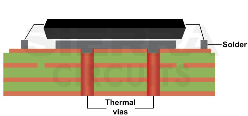
- Implement thermal relief pads on power components to improve heat dissipation and ease of soldering.
- Ensure that the enclosure or housing for your PCB and cooling fan is well-ventilated. Design openings or vents to allow for efficient airflow.
- Decide on the placement of the cooling fan on the PCB or within the enclosure. Ensure it is positioned to provide uniform airflow over critical heat-producing components.
- Dedicate large solid ground planes for thermal management of higher currents that act as heat sinks to distribute heat uniformly across the board.
For a deeper understanding of thermal management in circuit boards, read PCB heat dissipation techniques by Keven Coates.
9. Place components at a distance of approximately λ/10 from the board edge
Strategic PCB component placement plays a vital role in signal integrity in HDI boards. Placing critical components closer to each other can reduce signal path lengths, minimizing signal degradation and crosstalk. Carefully arranging signal routes, especially for high-speed communications, can improve signal integrity and minimize interference risk and crosstalk.
A few essential strategies for precise component placement in HDI PCBs to ensure robust signal integrity are:
- Abstain from placing sensitive high-speed components at the edge of the board to avoid radiation, electromagnetic interference, and the introduction of random capacitance. A recommended practice is to place these components at a distance of approximately λ/10 from the board edge. λ is the wavelength of the signal.
- Position heat-generating components away from sensitive components to prevent thermal issues and enhance reliability. Further, the placement strategy must ensure unrestricted airflow.
- Provide sufficient clearance between components to avoid accidental short circuits and for ease of assembly.
The table below summarizes the optimum spacing between various types of components:
| Chip | SOT | SOIC | PLCC | QFP | BGA | Axial | PTH | |
|---|---|---|---|---|---|---|---|---|
| Chip | 10-20 | 15-25 | 20-25 | 50-75 | 50-120 | 75-120 | 50-75 | 50-75 |
| SOT | 15-25 | 15-25 | 20-25 | 50-75 | 50-120 | 75-120 | 50-75 | 50-75 |
| SOIC | 20-25 | 20-25 | 30-50 | 50-100 | 75-120 | 75-120 | 50-75 | 100-150 |
| PLCC | 50-75 | 50-75 | 50-100 | 100-120 | 100-120 | 100-120 | 100-150 | 100-150 |
| QFP | 50-120 | 50-120 | 75-120 | 100-120 | 100-120 | 75-120 | 100-150 | 100-150 |
| BGA | 75-120 | 75-120 | 75-120 | 100-120 | 75-120 | 100-120 | 100-150 | 100-150 |
| Axial | 50-75 | 50-75 | 50-75 | 100-150 | 100-150 | 100-150 | 100-150 | 100-150 |
| PTH | 50-75 | 50-75 | 100-150 | 100-150 | 100-150 | 100-150 | 100-150 | 100-150 |
| **Dimensions given in this table are specified in mils | ||||||||
- Place components in close proximity on a circuit board to achieve shorter signal paths and reduced trace lengths. As a result, this helps maintain consistent impedance and reduces the chances of signal distortion, crosstalk, and other interference issues.
10. Maintain equal trace lengths for clock signals
High-speed clocks, crucial for system synchronization, require extra consideration to ensure signal integrity. Clock signals should be routed in such a way that clock skew is minimized, avoiding timing issues.
Proper clock signal routing and skew minimization for clock signals are critical for ensuring accurate timing and reliable system operation.
- Maintain equal trace lengths for clock signals to ensure synchronous data transmission.
- Avoid branches to minimize reflections. Instead, utilize a clock driver for distributing the signal to every device and consider a proper termination.

- Use impedance-matching resistors on the clock signal to match the output impedance of the clock driver to the characteristic impedance of the traces to ensure the clock signal integrity.
See what Syed Ubaid Ali Warsi, an expert in high-speed designs and an EMC consultant, has to say about high-speed and HDI design strategies.
About Pooja Mitra : Pooja Mitra is an electronics and communication engineer. With an experience of over three years in the PCB industry, she creates industry-focused articles that help electrical and PCB layout engineers.


In HDI PCBs, where traces outside the BGA region have a standard width and spacing of around 4 mil, what is considered an acceptable deviation in trace width and spacing when breaking out a BGA? How can you ensure that the transition from the BGA region to the rest of the PCB maintains signal integrity while accommodating the necessary changes in trace characteristics?
What termination techniques do you find the most effective for high-speed signals in HDI PCBs, and how do you determine the appropriate termination method?
Generally I think parallel is the default if you have no information. As far as determining the best method you should go by the components data sheet.
For component ingress and egress the discontinuities should be limited to Lambda/10.
By measuring it, preferably with a VNA.
Follow “Best Practices”