Contents

On-demand webinar
How Good is My Shield? An Introduction to Transfer Impedance and Shielding Effectiveness
by Karen Burnham
We recently worked on a PCB design comprising 2 modules. Module 1 has a microcontroller, and module 2 hosts antenna signals. These boards are connected through a hermaphroditic connector, which is generally used to distribute power among two circuit boards.
In this case study, you’ll learn the challenges we encountered in this design and how we resolved them. From addressing the connector alignment hurdles to optimizing component placement for efficient power distribution, we tailored the design and successfully integrated a microcontroller and a functional PCB.
Highlights:
- Module 1 has 3 power sources. Placing them on a compact board and ensuring efficient power distribution was challenging. To overcome this hurdle, we placed the sources sequentially and grouped the components as per their power requirements.
- Module 2 has antenna signals. Accommodating them in the layout resulted in space constraints. Our designers implemented coplanar traces to route the antenna signals, leaving enough space to route other signals.
Module 1: Microcontroller PCB
Customer’s design requirements:
- Total number of layers: 10
- Board thickness: 62 mil
- Board dimension: 3.5 x 2.5 inches
- Microcontroller: 196-pin MAPBGA, 12 x 12 mm, and 0.8 mm pitch (generally used in smart kitchen appliances)
- Build class: IPC-6012 class 2
- Connectors and power supply: USB, ethernet, batteries, power source, controller IC, and board-to-board connector.
- Finish copper thickness: 1 Oz on all layers
- Laminate (dielectric material): FR-370 HR
- Surface finish: ENIG
- Signal lines: 50 Ω single-ended controlled impedance traces of width ranging from 4.6 to 7.6 mil; 90 Ω and 100 Ω differential pair controlled impedance traces of 4 to 8 mil wide
- Processor: i.MXRT1060 Arm cortex M7 core 600 MHz processor with 0.8 mm pitch. The processor has chip RAM of 1 MB and operates at 3.3 V. This processor is specifically useful for applications such as industrial human-machine interfaces (HMI), motor control, and home appliances.
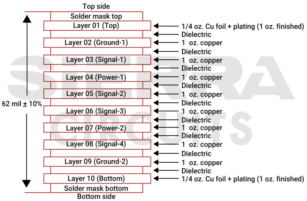
Stack-up configuration of this microcontroller circuit board
Module 1 has a symmetrical circuit board stack-up, comprising ground, signal, and power planes.
PCB layout challenges in Module 1
- Since the microcontroller incorporates 3 power sources, strategically placing the circuit board components on a compact 3.5 x 2.5-inch board area was crucial for efficient power distribution.
- The high-pin count of the BGA requires efficient routing strategies and should be placed away from the power sources.
These two problems are addressed below in solution 1 and solution 2, respectively.
Resolving layout issues in Module 1
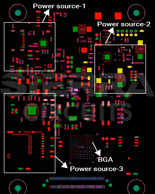
Solution 1: We segregated the components based on their power requirement and grouped them into sections in the circuit.
We followed a hierarchical sequence to arrange the power sources (USB, battery, and ethernet connector) shown in the layout below to ensure sequential flow and minimize power routing complexities.
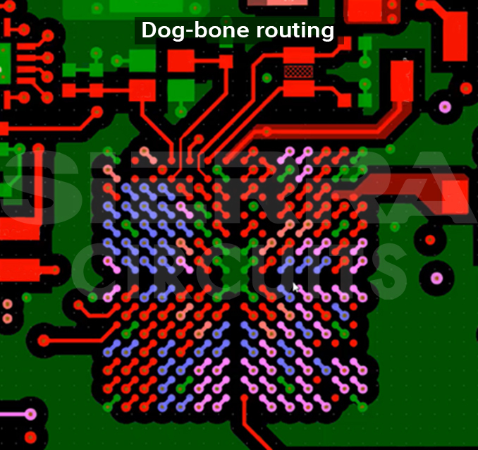
Solution 2: The BGA section was isolated from the power sections to ease the routing process. Ground vias were placed around the BGA section to provide shielding against EMI. This approach prevented components from being either too distant or too close to the BGA, contributing to effective power routing and component placement.
We maintained a clearance of 8 mil among all the components and implemented the dog bone fanout style to route the BGA.
To learn more about controlled impedance traces, download our Controlled Impedance Design Guide.

Controlled Impedance Design Guide
6 Chapters - 56 Pages - 60 Minute ReadWhat's Inside:
- Understanding why controlled impedance is necessary
- Stack-up design guidelines
- How to design for impedance
- Common mistakes to avoid
Download Now
Module 2: Functional PCB
Customer’s design requirements:
- Number of layers: 6
- Thickness: 62 mil
- Dimension: 3.5 x 2.5 inches
- Class: IPC-6012 class 2
- Dielectric material: FR370HR
- Surface finish: ENIG
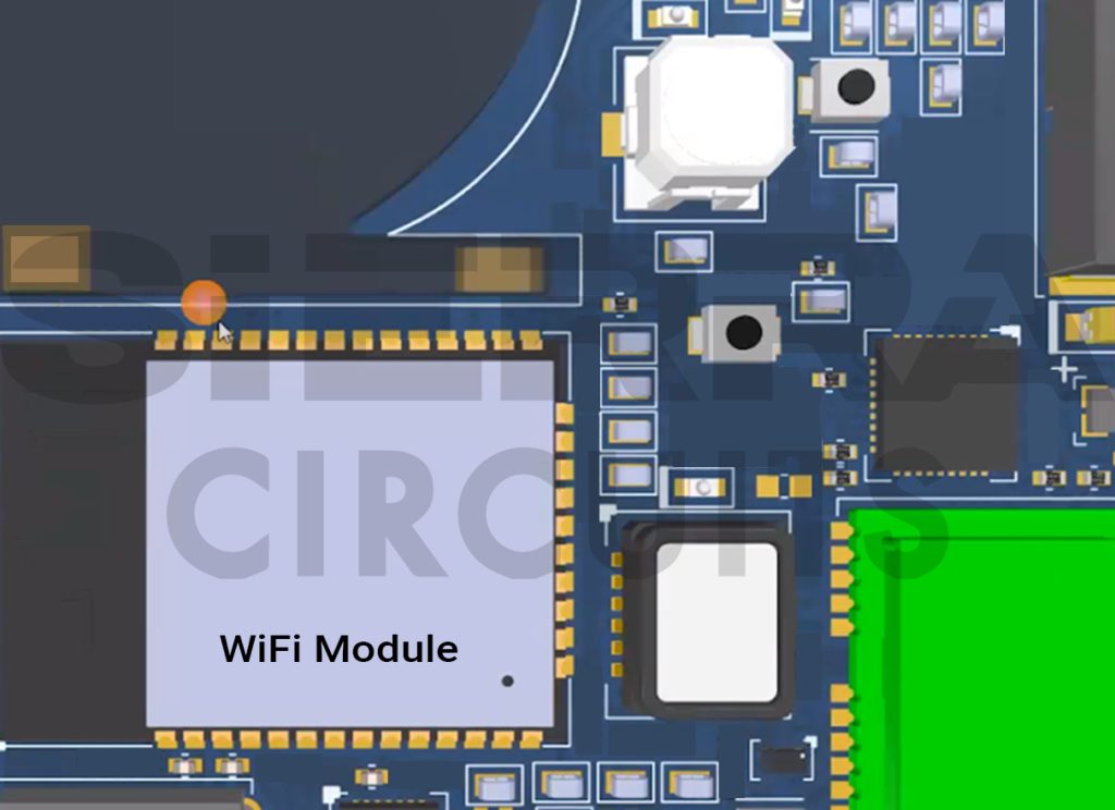
- Components/connectors: Pressure sensors, microphone, alert switch, battery, inclinometer, LEDs, USB, WiFi antenna, battery switch, inertial measurement unit, speaker, and board-to-board connector.
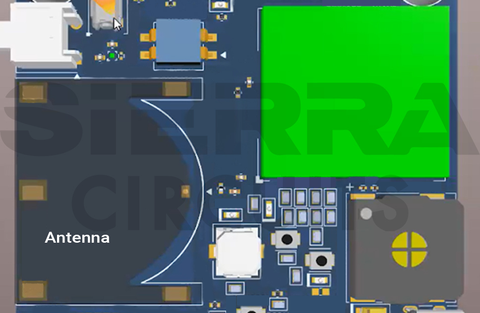
Finish copper thickness: 1 Oz. - Antenna: LARA-R6, operating at 1.9 GHz with voltage and current ratings of 2.8 – 4.5 V, and 50-630 mA, respectively.
- Signal lines:
- 50 Ω coplanar single-ended controlled impedance traces with trace width and spacing of 8.10 mil and 6 mil, respectively.
- 50 Ω single-ended controlled impedance traces with trace widths ranging from 5-9.8 mil.
- 90 Ω differential pair controlled impedance traces, with trace widths and spacing ranging from 4.5 to 7 mil and 5 to 5.5 mil, respectively.
- WiFi module: Operating at 2.5 GHz with a voltage range and maximum current of 3 to 3.6 V and 40 mA, respectively.
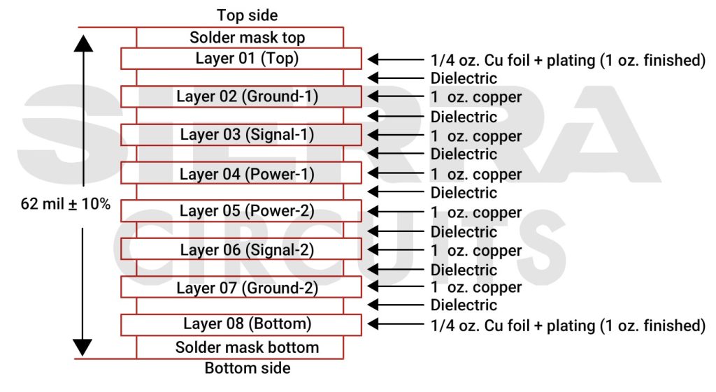
Stack-up configuration of the functional board
The customer had requested a six-layer board. Later, our designers decided to increase the number of layers to 8.
Resolving layout and interface issues in Module 2
- Aligning the connection point between the microcontroller and functional PCBs posed a challenge due to a unique 100-pin self-mating, hermaphroditic connector. This connector did not have a specific male or female side, which posed a significant automotive PCB layout challenge.

2. The customer initially requested a six-layer board, which proved unfeasible due to space constraints, anticipated current flow, and trace complexity.
3. Accommodating the antennas while leaving the space underneath empty on all layers.
These three issues are addressed below in solution 1, solution 2, and solution 3, respectively.
Overcoming the challenges in Module 2
Solution 1: We ensured precise alignment of connector coordinates to facilitate proper mating.
Solution 2: Responding to the customer’s initial request for a six-layer board, efforts were made to route and place all components within this configuration. However, upon evaluating the available space, anticipated current flow, and the complexity of the required traces, it became evident that accommodating all the specifications within six layers was not feasible. As a result, we decided to transition to an 8-layer board.
The decision to switch from a 6-layer to an 8-layer PCB design was not simply about adding more space; instead, it was a strategic move to address the optimal placement of many components with antennas involved. This helped us establish proper ground references throughout the board to facilitate effective power delivery, maintain trace width specifications, and isolate sensitive components from noisy sections.
Solution 3: The antenna specifications mandated leaving the space underneath copper on all layers, resulting in substantial unused space. This reduced the routing space significantly. We implemented coplanar transmission line models to route all the antenna signals with guard signals around them.
The coplanar transmission line model involves ground planes on either side of the signal trace. This arrangement creates a controlled environment for the signal, minimizing EMI. As a result, adjacent areas of the board can be utilized for routing differential pairs, without sacrificing signal integrity.
To learn what causes signal integrity problems, see 9 factors that lead to signal integrity issues in a PCB.
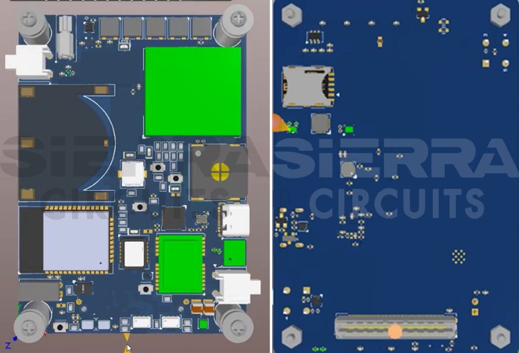
All aspects, including the component footprints and PCB schematic, were thoroughly verified. However, due to the unavailability of a vibrating motor, the client changed the MPN at the last moment.
During the final review process, we recognized a polarity mismatch associated with the altered MPN and fixed it. This proactive approach was crucial in preventing an error from reaching the production stage.
Check out our comprehensive PCB design services. Our engineers prioritize performance, manufacturability, cost, and design for testability to ensure the best possible board at a fair price.
Key takeaways
- Segregating components based on power requirements, grouping them into sections with different power ratings, and adopting a hierarchical sequence for their placement can help achieve efficient power distribution.
- Isolating the BGA section from the power section and placing ground vias around the BGA section can prevent noise interference and improve power routing and component placement.
- Verification of components and their schematic connections, component footprints, and schematic symbols are necessary for preventing a critical error.
Through a collaborative effort and careful consideration of design details, our PCB designers successfully overcame the challenges posed by microcontrollers and functional PCBs. Consequently, they optimized the BGA microcontroller and function boards, meeting the client’s stringent space constraints while maintaining high-performance standards. The tailored configurations and meticulous routing strategies ensured smooth integration within the automobile equipment, providing improved functionality within limited spaces.
Need assistance in designing your board? Post your queries on our PCB forum, SierraConnect; our PCB experts will answer them.

Check out our series of design case studies, covering topics such as resolving EMI and PCB routing issues, routing microcontrollers in rigid-flex PCBs, and handling the complexities of HDI boards with BGAs.
About Mohamed Faheemuddin : Mohamed Faheemuddin is a mechanical engineer. His passion for electronics drew him to the PCB industry. With an experience of over 3 years in the PCB industry, he specializes in developing articles for engineers and hardware designers.







Start the discussion at sierraconnect.protoexpress.com