Contents

On-demand webinar
How Good is My Shield? An Introduction to Transfer Impedance and Shielding Effectiveness
by Karen Burnham
Keven Coates shared his insights about PCB heat management at PCB West 2023. Keven Coates, a senior electrical engineer in avionics, has been a speaker at PCB West for a decade now and has shared his expertise in optimizing heat management in circuit boards.
Highlights:
- Use thermal interface materials such as thermal pads and heat sinks on power MOSFETs, and LEDs to dissipate heat, effectively.
- While choosing MOSFETs, opt for larger packages (five-by-five and TO-220) to maximize the thermal dispersion.
- Select thicker copper (≃ 2 Oz) to spread out heat without any external materials.
Watch the full video to learn more.
Could you share some best practices for heat management in PCB designs with processors, power MOSFETs, and LEDs?
Keven Coates: When it comes to heat management, the key is to spread out the heat. If a substantial amount of heat concentrates in a small space, even a mere hundred milliwatts of heat can be a significant cause of concern. However, it’s no longer a crucial issue when you spread that heat out.
For instance, when you design processors, you need to employ methods to handle the heat by identifying the source of heat generation on the processor. In most cases, processors will require the application of thermal interface material, such as thermal pads, on top of the chip. Ideally, you’d want to incorporate a heat sink on it to dissipate heat efficiently.
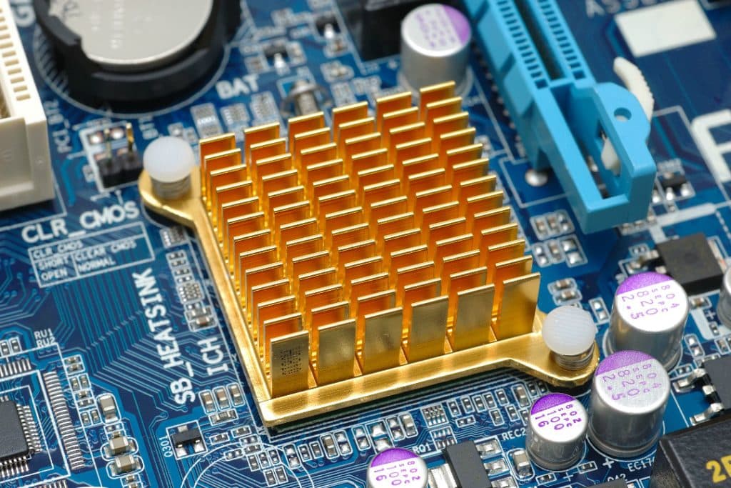
Using fans is not ideal in most cases because they tend to break down and pull in a lot of dust. It’s usually better to create a design that doesn’t rely on a fan. However, the choice really depends on the specific processor you’re working with. In rare cases, certain processors release heat through the bottom where the BGA ball connections are located. In such situations, you can use a heat sink on the bottom of the chip, which is more effective than placing a heat sink on the top.
Typically, the MOSFETs are high-power components, so always attach a heat sink to them. The preferred method is using a heat sink soldered around the device, which helps draw the heat away through the copper onto which the hot MOSFET is soldered. The heat sink then extends above the board, providing a larger surface area for more effective cooling. The same principle applies to LEDs, especially if you can use thick copper, like two-ounce copper, to spread the heat as efficiently as possible.
For valuable insights into various heat dissipation techniques in circuit boards, read 12 PCB thermal management techniques to reduce PCB heating.
How do you select appropriate materials to optimize heat dissipation in circuit boards?
Keven Coates: Preferably select materials that are readily available and don’t cost extra. For instance, two-ounce copper is a great choice. Design your board with this type of copper to efficiently spread out heat, needing no extra materials.
If you’re dealing with a component like a MOSFET that emits fifty watts of heat, you’ll require a significantly more robust heat management solution. It truly depends on the level of heat you need to dissipate effectively.
PCB Material Design Guide
9 Chapters - 30 Pages - 40 Minute ReadWhat's Inside:
- Basic properties of the dielectric material to be considered
- Signal loss in PCB substrates
- Copper foil selection
- Key considerations for choosing PCB materials
Download Now
Can you share a few component placement techniques to manage heat dissipation?
Keven Coates: PCB heat management revolves around maximizing the spread of heat as much as possible. One effective approach is to position heat-dissipating elements at the center of the board. A more efficient circuit board component placement technique is spreading components across the entire board. The decision heavily relies on whether you are dealing with a single component or multiple components that generate a substantial amount of heat.
For instance, placing MOSFETs in the corners of the board significantly limits the available space to disperse the heat. So, avoid corner component placements unless you have a well-planned strategy for utilizing a heat sink at the board’s edge.
What are the best strategies to integrate heat sinks and thermal vias in your PCB layout?
Keven Coates: There are indeed numerous types of heat sinks available, so it becomes a tough choice. Although, one of the most preferred approaches, particularly for MOSFETs, is to opt for larger packages. Tiny MOSFETs might boast excellent ratings for low resistance and power. However, their small size restricts the effective spread of heat. So, you need to opt for the larger package options, like a five-by-five or even a TO-220 MOSFET, depending on the power requirements.
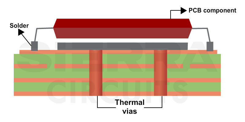
When working with a five-by-five MOSFET, you should prefer to use the thickest copper available to maximize heat dispersion. You can solder the heat sinks around the MOSFET to draw heat away effectively. Additionally, you can incorporate thermal vias adjacent to the MOSFET to facilitate heat transfer to the opposite side. If necessary, you can also attach an additional heat sink on the opposite side of the board for effective thermal dissipation. It all boils down to the idea of spreading the heat as far and wide as possible for optimal heat management.
What are some of the common issues designers face when working with high-power components?
Keven Coates: High-power applications indeed come with two key challenges. The first is managing heat, which typically involves using a heat sink or a similar solution. The second challenge is mitigating radiated emissions, which can cause issues depending on the frequency involved.
One effective strategy for emission control is managing the return paths. As current flows out of your high-power device, ensure that there is a nearby and well-designed return path. This helps minimize the size of the loop area for the high-power device. As a result, it prevents radiated emissions, which could introduce unwanted noise into nearby circuitry.
Why should PCB designers and engineers attend your upcoming webinar on heat management and high speed boards?
Keven Coates: If you are interested in learning more about heat management, especially dealing with components that generate around two watts or more of heat. It’s essential to acquire knowledge of fundamental techniques for effective heat dissipation. This includes understanding how to utilize copper and leveraging cost-effective methods on the circuit board for heat management. Signal integrity is another crucial aspect to consider when designing a successful board.
Having a firm grasp of both heat management and signal integrity will enhance your skills as a designer. In addition to this, it elevates your value in the industry. Major companies are actively seeking experts in signal integrity, so this knowledge can greatly benefit your career. Numerous PCB designers may not know these essential aspects, making it vital for you to be well-versed in them. Being well-versed in these areas can make you an exceptionally valuable asset.
Click here to watch the on-demand webinar.
Key takeaways:
- The most critical aspect of heat management is to disperse the heat across your circuit board.
- When designing processors, identify the sources of heat generation and use thermal interface materials like thermal pads and heat sinks to dissipate heat efficiently.
- Do not place the heat-generating components such as MOSFETs at the corner of the board. This minimizes the heat spread in the layout.
These design recommendations by Keven Coates can help you create better PCB thermal management strategies for your next design.
About Pooja Mitra : Pooja Mitra is an electronics and communication engineer. With an experience of over three years in the PCB industry, she creates industry-focused articles that help electrical and PCB layout engineers.




Start the discussion at sierraconnect.protoexpress.com