


Contents

On-demand webinar
How Good is My Shield? An Introduction to Transfer Impedance and Shielding Effectiveness
by Karen Burnham
Maintaining the highest quality standards in boards while simultaneously reducing PCB assembly costs can be an ongoing struggle for designers and manufacturers.
In this article, you will learn some advanced techniques for reducing circuit board assembly costs without compromising the integrity of the final product.
Highlights:
To reduce the PCBA cost:
- Clearly define component boundaries.
- Prefer SMDs as they are compatible with automated assembly.
- Choose standardized passive components such as 0201, 0402, 0603, and 0805.
- Opt for RoHS-compliant components.
Global and North American PCBA market projections (2023-2029)
The PCB assembly market is expected to grow significantly. This is driven by increased demand across various sectors, including electronics, automotive, telecommunications, healthcare, and industrial equipment.
Global PCB assembly market size

The global PCB assembly market is expected to grow from $96.75 billion in 2024 to $142.16 billion in 2029. The market is forecasted to grow at a CAGR of 6.6% during the forecast period.
Source: Sierra Circuits’ market research analysis report derived from the annual reports of PCBA industry leaders.
North American PCB assembly market size

Source: Printed circuit board association of America
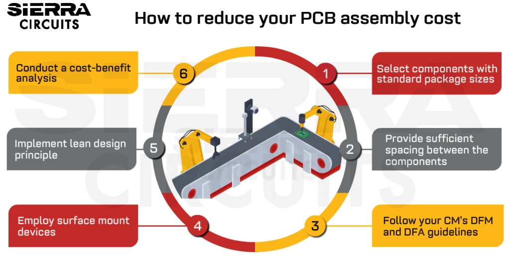
6 factors that impact your PCB assembly price

9 design tips to reduce circuit board assembly cost
1. Select components with standard package sizes to simplify the supply chain
Component selection is a critical aspect of printed circuit board design that can significantly impact the overall expense.
11 strategies for efficient part selection to reduce the assembly cost
- Choose components with standard package sizes (0201, 0402, 0603, and 0805) and footprints to streamline the product’s supply chain and reduce the need for custom circuit board layouts.
- Refer to the component datasheets and follow industry standards such as IPC-7351 when creating footprints. The land pattern must match the dimensions to ensure reliable soldering and electrical connections.
- Ensure pads are appropriately sized and spaced to prevent misalignments and interference between adjacent components.
- Accurately define the part outline to avoid errors during the automated assembly procedure. Errors in sizing may require manual intervention, potentially increasing the board’s cost.
- Check the availability and lead times of components from different manufacturers and suppliers.
- Parts with long lead times or limited availability can result in production delays and increased costs due to component scarcity.
- Optimize component selection based on their lifecycle status during the design phase. If a critical component reaches the end of its lifecycle before production begins, it causes disruption, leading to delays and the need for reengineering.

To avoid stockouts, lifecycle risks, and last-minute redesign costs, see the PCB procurement checklist for hardware engineers.
-
- Check for component availability before sending the design files to the fabrication house. This is critical as some parts might be out of stock at the time of ordering them.
To eliminate potential supply chain disruptions, Sierra Circuits offers PCB component sourcing and stocking facility called customer-owned inventory. Here, we handle your components from quoting to assembly.
- Include alternate part numbers in your PCB bill of material for items that might go out of stock. This helps save time on substitution approvals early on in the process.
- Be flexible with component values wherever possible and communicate this flexibility to your fabricator. This ensures that minor variations in component values do not disturb your design.
- While designing your circuits, consider the tolerances of components like resistors, capacitors, inductors, and diodes. Components with wider tolerances are cost-efficient. Typically, the tolerances for resistors are 0.1%, 1%, 5%, and 10% of their value.
- Do not choose overspecified components, as they can complicate the procurement process and increase the cost and lead time.
- Check for alternative components available in the market that may offer similar or superior performance at a fraction of the cost. Conducting an in-depth analysis of component options is essential for price-conscious PCB designers.
- Minimize the number of components by using multi-functional circuits wherever possible.
- Clearly mention DNI components in your BOM. DNI is generally assigned to components involving larger or heavier objects, such as high-valued electrolyte capacitors.
- Always choose RoHS-compliant parts. Non-RoHS-compliant components, such as BGAs, must be re-balled to meet RoHS requirements, which escalates the assembly price. Further, if you want to design a board that includes both RoHS and non-RoHS components, it requires a hybrid assembly, which is a costly affair.
- Check if the selected components are available in reel packaging. Manufacturers often offer reels for components with high demand, ensuring cost-effectiveness.
To learn how to avoid assembly delays and extra costs, download our design guide.

PCB Design for Assembly Handbook
6 Chapters - 50 Pages - 70 Minute ReadWhat's Inside:
- Recommended layout for components
- Common PCB assembly defects
- Factors that impact the cost of the PCB assembly, including:
- Component packages
- Board assembly volumes
Download Now
2. Provide sufficient component spacing to prevent solder bridging
Placing components in close proximity could cause difficulties in soldering, inspection, and assembly processes due to limited access or interference between components.

11 key design tips for component placement to ensure PCBA cost efficiency
- Define minimum placement courtyards for components, preventing solder issues and aiding assembly. Use the manufacturing zone for rework, ensuring accessibility. Maintain 0.25 mm clearance, with exceptions: 1.0 mm for BGA, 0.15 mm for parts smaller than 0603 packages, and 0.5 mm for connectors, crystals, canned capacitors, and connector mating.

- Provide sufficient part-to-part spacing to facilitate easier manual soldering or rework while recognizing form factor requirements. While greater spacing eases assembly, some applications, particularly those aiming for a smaller form factor, may necessitate closer spacing. Balance these factors based on the project’s goals.

- Place IC sockets away from sensitive packages to minimize stress on nearby solder joints caused by repeated plugging and unplugging. This practice enhances the longevity and reliability of the connections. In addition, you need to select relevant PCBs for IC integration to ensure desired performance.
- Avoid placing sensitive component packages in the center of the PCB. The central region may experience bow and twist at maximum intensity, leading to broken connections. Distribute sensitive components strategically across the board.

- Practice increasing the component-to-board edge spacing on the board. This helps accommodate hold-down clamps used during the solder application process, preventing potential blockage of surface-mount components and avoiding damage during assembly. Also, components near the board edge can be subjected to stress during depanelization, potentially compromising solder joints.
-
-
- Install larger components at a distance of 125 mil from the edge of the board
- Place smaller components 25 mil away from the board’s edge.
-

- Recognize that clearances for automated assembly processes and manual assembly processes differ. In manual assembly, components can be placed closer to the edge post reflow and depanelization. Adjust the design accordingly based on the chosen assembly method.
- Ensure that both copper traces and manually installed parts are distanced at least 10 mil from the edge of the board. This distance allows for a solder mask gap and prevents pad encroachment, contributing to the PCB’s overall reliability.
- In designs requiring copper plating at the board edge, such as those incorporating castellated holes, be aware that achieving the desired copper plating may involve additional cost and lead time. Factor this into the design considerations and project timelines.
- Be cautious placing surface-mount components in the areas affected by hold-down clamps during the solder application process. Blocking by clamps could result in inadequate solder paste application or potential damage to SMT components.
- Maintain a minimum of 8 mil spacing between the hole edge and the component pad’s edge to prevent unintended connections. For manual soldering, this ranges between 50 to 100 mil

- Keep a minimum of 7 mil space between the edge of the component pad to the edge of the annular ring. However, this can be between 50 to 100 mil for manual soldering.
-
-

Maintain a minimum of 7 mil component to annular ring spacing
-
For more, see component placement guidelines for PCB design and assembly.
3. Adhere to DFA standards to minimize the turnaround time
DFA rules focus on optimizing the ease of assembling components onto the board, reducing production costs, and improving overall manufacturing efficiency.
9 DFA techniques to cut down printed board assembly price
- Resist the temptation to overpopulate your circuit board. Overcrowding can make component placement and soldering more challenging, leading to increased assembly time and costs.
- Stick to regular board shapes, such as rectangles or squares, whenever possible, as irregular shapes can affect the panelization method used, complicate the assembly process, and increase costs.
- Consider the operating environment of the board. PCBs exposed to substantial vibrations require through-hole components because they offer a more secure attachment compared to surface mount devices.
- Employ sufficient thermal relief. This ensures the creation of high-quality solder joints and eliminates specific soldering issues.
- Implement effective trace routing methods. Misalignment of traces with pads or vias could lead to insufficient solder connections and need rework.
- Adhere to the size, spacing, and tolerances for drill holes that fall within your fabricator’s capabilities. This practice guarantees the design’s manufacturability.

- Avoid edge mounting or hanging components to increase the number of printed boards on the array during assembly. If the component is within the board, then the number of PCBs on the assembly array will increase, decreasing assembly cost.

- Ensure that components are accessible for soldering and inspection to avoid difficult-to-reach or hidden components that can lead to errors and rework, increasing the assembly cost.
- Verify component footprints against datasheet specifications during the design phase to avoid mismatch errors. Engage with your PCB assembly partner early in the design phase to leverage their expertise in this matter.
During a routine DFA check of a circuit board design provided by a customer, our PCB assembly engineers discovered a footprint mismatch. The mechanical dimensions of the component (FB115) in the Gerber did not match the datasheet.
The Gerber files indicated a pad footprint for a 1005 package, whereas the actual component was a 0805 package. This inconsistency raised concerns about potential assembly issues and unnecessary expenses.

We immediately initiated a thorough review of the design files and collaborated with the client to rectify the issue.
The proactive detection and resolution of the footprint mismatch avoided potential assembly errors, associated costs, and production delays.
Sierra Circuits performs a thorough DFA analysis to ensure error-free PCBA. Upload your BOM to get an online quote.
4. Follow DFM guidelines to ensure manufacturability
DFM involves designing the printed board layout with the manufacturing process in mind, making it easier, more efficient, and cost-effective to produce.

7 DFM techniques to reduce your circuit board assembly expense
- Group components based on their functions and connections to reduce trace lengths and reduce crossover routing. This minimizes the complexity of the board layout and reduces assembly and manufacturing time and errors.
- Consider placing BGA and other SMTs on only one side of the board to facilitate a single reflow soldering step followed by the mounting of through-hole components with wave soldering or manual soldering. This eliminates the need to reposition the board for double-sided assembly reducing costs associated with flipping and aligning the PCB.

- Ensure SMT components are not positioned one beneath the other with the same XY coordinates if the placement of SMTs on both sides is unavoidable. This prevents complications in X-ray inspection and rework processes.

- Reduce the number of board layers to decrease material costs, PCB drilling, lamination, and assembly expenses. Careful layer planning can help you strike the right balance between cost and functionality.
- Ensure that components are clearly marked with reference designators and values to avoid confusion during assembly. This reduces the risk of misplacement and errors.
- Reuse successful PCB designs for similar projects, saving both design and assembly costs.
- Collaborate with manufacturing partners to conduct a thorough DFM assessment. Identify design elements that may hinder efficient assembly or increase costs, and work together to make necessary adjustments.

5. Employ SMDs for rapid and precise component placement
SMDs are directly placed onto the surface of the PCB, as opposed to through-hole components that are inserted through drilled holes. This technology offers several advantages that contribute to cost efficiency.

5 SMT design strategies to improve cost efficiency in PCBA
- Choose SMT components that are cost-effective, readily available, adhere to standard package sizes, and are more compatible with automated assembly. Using a consistent set of components across different products can lead to bulk discounts. Also, standardized packages are compatible with automated assembly processes.

Surface mount and through-hole resistors 
Surface mount and through-hole capacitors - Ensure that your designs accommodate SMT components using surface-mount footprints rather than through-hole footprints. This eliminates the need for additional modifications and reduces production time.
- Avoid using fasteners as they drive up PCB assembly costs. Instead, use SMDs for power ICs along with heat sinks.
- Carefully plan the placement of SMT components on the PCB by grouping components logically based on function and signal flow to reduce the travel distance of assembly equipment.
- Reduce the number of SMD variants used in your designs to simplify the procurement process and minimize inventory management challenges faced by component procurement experts.
For THT components, see through-hole assembly design rules.
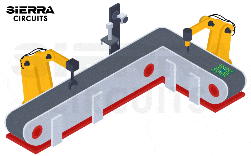
6. Prioritize design for automation to streamline the pick-and-place process
Design your boards with automated assembly in mind, which includes clearly defining component orientation and ensuring proper spacing. An assembly-friendly design minimizes the risk of errors during the automated pick-and-place process. Automated assembly aims to reduce assembly costs of PCB, minimize component inventory, and improve the quality and reliability of the assembly process.
In preparation for automated assembly, it is necessary to utilize components of consistent quality. These components should adhere to precise geometric and dimensional tolerances to minimize the risk of assembly defects due to component mismatch.
Further, high-speed memory modules (e.g., DDR5), AI processors, and advanced LiDAR sensors demand precise placement, as any misalignment can cause signal interference, reducing processing efficiency. To achieve this, robotic-assisted surface-mount technology (SMT) is used to ensure micron-level accuracy in component placement for humanoid robotics PCBA.
5 tips for seamless assembly automation
- Opt for components that snap together (press fit) wherever possible.
- Minimize angular component orientations to simplify the pick-and-place process. Some automated machines may require additional setup time for rotated components, which can slow down the assembly process and increase the risk of errors.
- Minimize the number of fasteners used in the assembly. Instead, use self-aligning and self-locating features that include guide pins, dimples, and chamfers. Ensure the screw heads used are consistent throughout the design if fasteners cannot be excluded.
- Every component selected during the design should be able to withstand the forces that will be exerted during the automated assembly process
- Choose components that can be oriented easily to reduce the turnaround time, resulting in cost and time savings. This will eliminate or at least reduce the requirement of reorienting stations before being fed to the assembly line.
7. Implement DFT rules to ease the testing process
Design for testing involves including designated test points on the board to facilitate testing during manufacturing and operation. DFT helps our PCB testing engineer to identify and rectify issues early in the design phase, reducing overall assembly time.
13 design for testing rules to eliminate board respins
- Place one test point per net, upstream and downstream, in your design to facilitate testing and debugging during assembly.

- Label key test points on the PCB to indicate their intended purpose and function, which helps reduce testing time and potential errors.
- Opt for a standard class 2 instead of class 3 when you are designing a circuit board for devices like laptops, smartphones, and tablets. Class 3 is reserved for military and medical applications, which come with more demanding specifications and stringent regulations. By following Class 2 standards, you can significantly cut down your project expenses.
- Follow the same principle that holds true when it comes to assembling circuit boards. For surface-mount component placement, the cleanliness requirement rules vary between class 2 and class 3, and adhering to these distinctions can impact your project’s costs.
- Ensure that components and test points are physically accessible using testing probes or fixtures. Avoid placing components in hard-to-reach locations, and provide ample space around test points.
- Incorporate dedicated probe pads or test points at strategic locations, including critical signal nodes, power rails, and key interfaces, to facilitate efficient electrical testing without the need to physically probe components.
- Implement boundary-scan (joint test action group or JTAG) capabilities in the PCB design. This allows for comprehensive testing of components and interconnections without direct physical access, reducing the need for complex test fixtures.
- Design certain board components or subsystems with built-in self-test (BIST) features. These components can perform self-diagnostic tests upon startup, helping identify defective parts before the assembly process, thus reducing rework costs.
- Include test access ports (TAPs) for JTAG or other testing protocols that enable external test equipment to connect to the PCB for debugging and testing purposes.
- Use silkscreen markings to indicate component polarities, pin numbers, and critical information that testers need to know during the assembly and testing processes.
- Use a 0.050-inch (not smaller than 0.025 inches) font size for best results.
- Keep the font’s line width higher than 0.005 inches.
- Place reference designators close to their part and preferably rotate it by 90 degrees to improve readability.
- Place silkscreen at a minimum distance of 0.005 inches from PCB pads and other features.

- Ensure that the printed board layout accommodates in-circuit testing. This involves designing test points and access areas that allow testers to make contact with specific components or traces using specialized ICT fixtures.
- Include dedicated test points for measuring voltage and ground throughout the board. This helps identify power delivery issues, short circuits, or voltage irregularities.
- Design the circuit board layout to accommodate flying probe testing. Ensure that the flying probe test system can easily access key test points and critical signal nodes, making the testing process more efficient. This method is known to be highly cost-effective for prototypes with low to mid-sized production runs.

To learn how to design a cost-efficient PCBA without board respins, download our handbook.

Design for Testing Handbook
7 Chapters - 28 Pages - 45 Minute ReadWhat's Inside:
- PCB testing strategies
- Guidelines to design and place a test point for FPT
- Directives to make your board ICT compatible
- Benefits and drawbacks of various testing methods
- Defects that you can identify through board testing
Download Now
8. Employ the lean design principle to eliminate part wastage
Lean design is a systematic approach that seeks to eliminate waste, optimize processes, achieve cost-efficiency, and enhance product quality throughout the PCB design lifecycle.
8 lean design principles to minimize PCBA cost without compromising quality
- Simplify designs whenever possible by reducing unnecessary features, complicated routing, and over-specified components. Lean designs are inherently easier and more cost-effective to assemble.
- Arrange components logically based on the assembly sequence to minimize the risk of errors during assembly and testing.
- Optimize trace spacing to reduce the size of the PCB board. With a smaller board size, pick-and-place machines and soldering equipment can operate faster and with higher precision, leading to reduced labor costs and shorter assembly times.
- Minimize the usage of non-washable components such as microphones, relays, switches, and memory chips to reduce the assembly cost.
- Non-washable components can only be assembled after the assembly of the complete board, which requires additional manual activity that leads to increasing the overall assembly cost.
- Washing the complete board can be skipped passing on to reflow soldering without cleaning the board if the board is not designed for high frequency application.
- Embrace the Kaizen philosophy of continuous improvement to refine design processes over time.
- Implement standardized design and processes and reduce variability to enhance consistency, reduce errors, improve efficiency, and maintain a stable and predictable design workflow.
- Design based on customer demand to avoid overproduction and unnecessary costs.
- Collaborate with manufacturers on sustainability practices, such as recycling and waste reduction, to minimize disposal costs.
9. Conduct a cost-benefit analysis to evaluate potential expense reduction
Performing a cost-benefit analysis ensures the design decisions are both cost-effective and aligned with project goals.
11 steps to conduct a cost-benefit analysis for your PCB assembly
- Clearly define your specific cost reduction objectives if you are aiming to reduce component costs, labor costs, or overall manufacturing costs, which will guide your analysis.
- Break down the cost components associated with PCB assembly. These typically include
- Component costs (e.g., resistors, capacitors, ICs).
- Labor costs (e.g., assembly, soldering, inspection).
- Material costs (e.g., printed circuit board, solder, adhesives, hardware).
- Overhead costs (e.g., facility costs, equipment maintenance).
- Identify potential assembly price reduction strategies, as discussed in the above sections, that can be applied to your board design.
- Estimate the potential savings associated with each cost-reduction strategy. Use historical data, quotes from suppliers, or industry benchmarks to obtain accurate cost figures.
- Evaluate the complexity and feasibility of implementing each cost-reduction strategy. Some strategies may require design changes, while others may involve changes in the manufacturing process or supplier relationships.
- Consider the risks associated with each price reduction strategy. Will the changes introduce new reliability or quality issues? Assess the impact of these risks on the overall project.
- Assess any trade-offs between cost reduction and other design considerations, such as performance, quality, and time-to-market. Determine whether any compromises are acceptable.
- Based on your analysis, prioritize the price reduction strategies that offer the most significant benefits with manageable risks.
- Consider the overall impact of the cost reduction methods on the project budget, schedule, and performance goals.
- Document your analysis, findings, and decisions. This documentation can be valuable for project stakeholders, including management and manufacturing teams.
- Continuously monitor and evaluate the effectiveness of the implemented cost-reduction strategies. Make adjustments as needed to achieve ongoing cost savings.
To reduce assembly costs, choose PCB component management services. Here, your fabricator handles procurement and storage of all the required parts.
Key takeaways:
- Maintain consistent footprint sizes and shapes for simplified assembly.
- Provide ample part-to-part spacing to avoid fabrication errors and facilitate manual soldering.
- Avoid overpopulating the PCB to reduce assembly time and costs.
- Design consistent component orientations to streamline the assembly process.
- Minimize component rotation angles for simplified pick-and-place processes.
- Opt for components that can snap together to minimize fasteners and reduce assembly time.
- Include designated test points and labels for efficient testing and debugging.
Need help designing a cost-efficient circuit board? Post your questions and get them answered by PCB experts on our forum, SierraConnect.
About Pooja Mitra : Pooja Mitra is an electronics and communication engineer. With an experience of over three years in the PCB industry, she creates industry-focused articles that help electrical and PCB layout engineers.


How does the choice of surface finishes impact the overall cost of circuit board assembly?
How can the choice of panelization technique impact the overall cost of PCB assembly?
Surface finishes range in cost, cheapest will be HASL or lead free HASL. It then increases from Enig-Enepig-Soft/Hard Gold (the more gold needed the higher the cost).
To stay lower cost, let Sierra panelize the job. We currently have a customer who is trying to panelize to maximize the space for lower cost, but it’s leading to warpage.